Photoelectric converter and manufacturing method thereof, and photoelectric conversion module

a technology of photoelectric converter and manufacturing method, applied in the direction of photovoltaics, electrical devices, semiconductor devices, etc., can solve the problems of degrading the photoelectric conversion efficiency of the photoelectric converter, unable to achieve low resistance,

Inactive Publication Date: 2012-06-28
MITSUBISHI ELECTRIC CORP
View PDF2 Cites 26 Cited by
  • Summary
  • Abstract
  • Description
  • Claims
  • Application Information

AI Technical Summary

Benefits of technology

[0008]It is an object of the present invention to at least partially solve the problems in the conventional technology.

Problems solved by technology

However, in the junction with p-type Si, the junction becomes an n-p junction, and thus a low resistance can be hardly achieved.
Therefore, even if a conductive film made of these materials is used, particularly when an electric current generated by the photoelectric conversion layer that concentrates light to generate power is large, the conductivity of the electric current is restricted by the resistance of the intermediate layer, thereby causing a problem such that the photoelectric conversion efficiency of the photoelectric converter is degraded.

Method used


Image

  • Photoelectric converter and manufacturing method thereof, and photoelectric conversion module
  • Photoelectric converter and manufacturing method thereof, and photoelectric conversion module
  • Photoelectric converter and manufacturing method thereof, and photoelectric conversion module

Examples


first embodiment

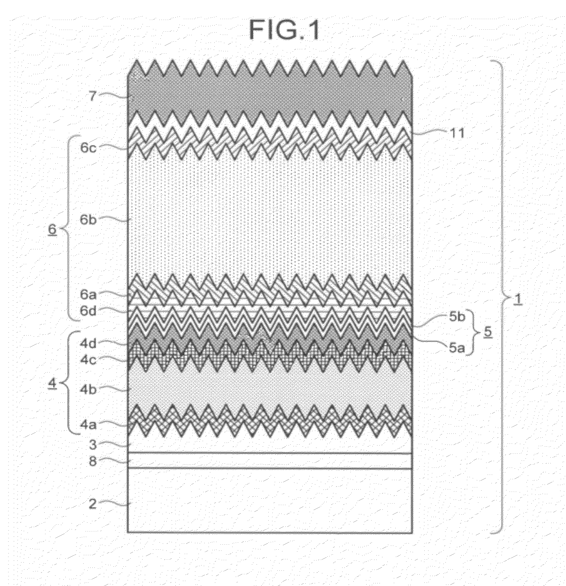
[0017]FIG. 1 is a sectional view of a schematic configuration of a photoelectric converter according to the present invention. In FIG. 1, in a photoelectric converter 1, a transparent electrode 3 having a surface texture structure with fine irregularities, an amorphous Si photoelectric conversion layer 4, an intermediate layer 5, a microcrystalline Si photoelectric conversion layer 6, and a backside electrode 7 are sequentially stacked on a substrate 2 having insulation properties and translucency. Further, as an impurity inhibition layer, an undercoat layer 8 can be formed on the substrate 2 as required. As a material of the undercoat layer 8, a silicon oxide film can be used.

[0018]The amorphous Si photoelectric conversion layer 4 and the microcrystalline Si photoelectric conversion layer 6 include Si as the main component thereof; however, have a different bandgap due to a difference in a crystalline structure, and therefore have different light-absorbing wavelength characteristic...

second embodiment

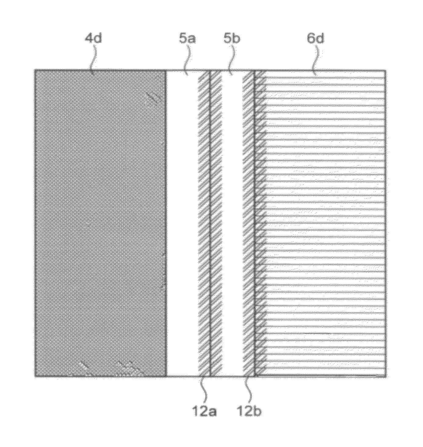
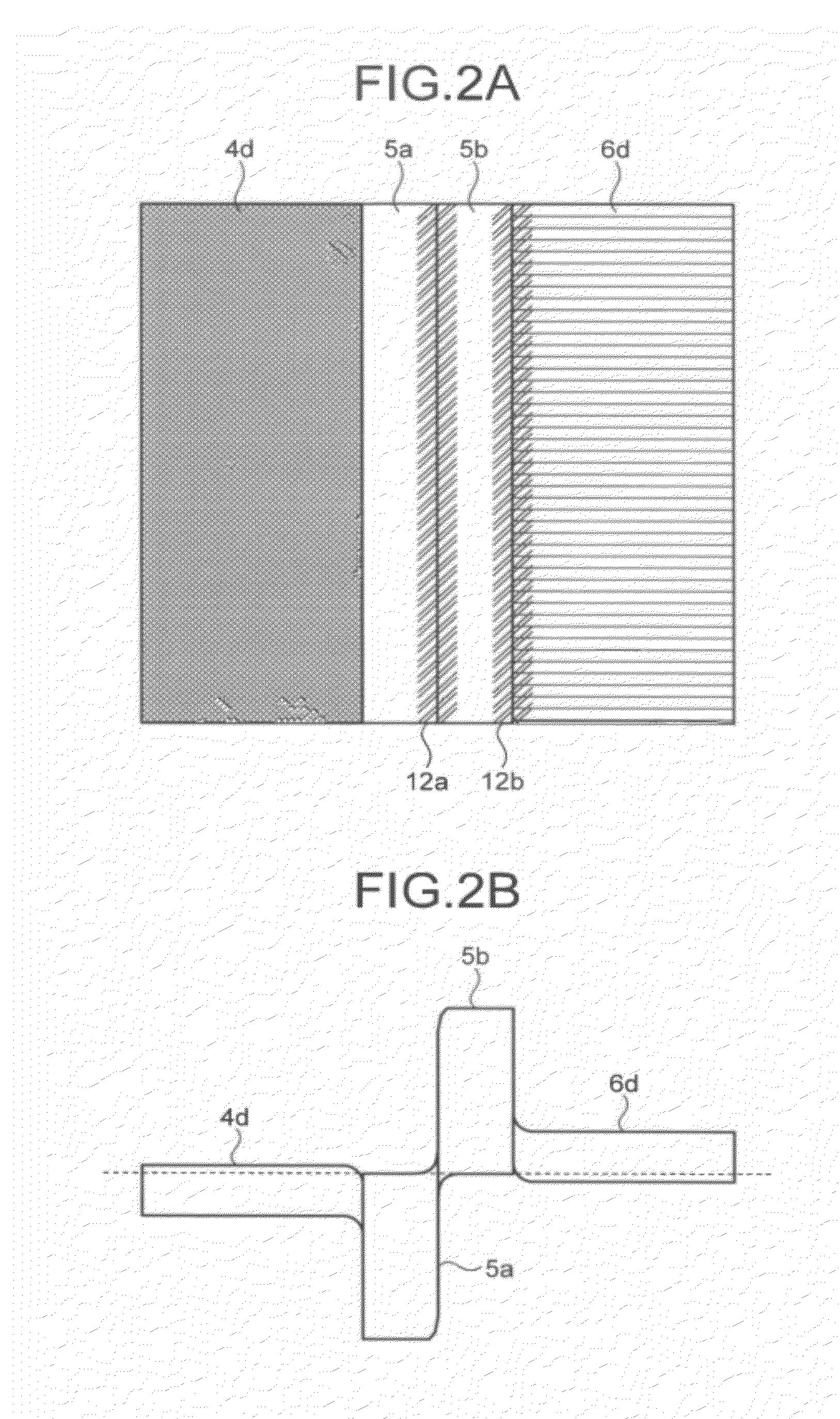
[0062]In the intermediate layer 5 having such a configuration, an electric current flowing between the amorphous Si photoelectric conversion layer 4 and the microcrystalline Si photoelectric conversion layer 6 is determined mainly by tunneling conduction and carrier recombination. Because the Al-doped ZnO and ZnIr2O4 used for the intermediate layer 5 are transparent conductive films, the original conduction characteristic is not affected much by the film thickness. However, when high-temperature heat treatment described here is not performed after film formation, the original mobility is not always realized sufficiently. Therefore, it is preferable to have a small film thickness.

[0063]An effect of the intermediate layer 5 is explained next. A Schottky junction between an n-type Si layer and an Al-doped n-type ZnO layer (n-type ZnO:Al) has a small Schottky barrier, because respective potential positions in a conduction band (an electron affinity) are close to each other. Therefore, ...

seventh embodiment

[0094]In the formation of the intermediate layer 5 described above, in film formation of each layer near the interface between respective layers, the surface of a previous layer is exposed to film formation of the next layer in different film forming conditions. Therefore, the vicinity of the interface may be affected by film formation of the next layer to have a high resistance. Therefore, in the present invention, in the forming method of the intermediate layer 5 described above, RF power to be applied at the time of film formation of the p-type transparent conductive oxide film 5b by the RF sputtering method is changed in two or more stages.

[0095]For example, when the p-type transparent conductive oxide film 5b is to be formed on the n-type transparent conductive oxide film 5a by the RF sputtering method, the RF power to be applied is set to 50 watts at the time of film formation for 2 nanometers of film thickness close to the interface with the n-type transparent conductive oxid...


PUM


Abstract

A photoelectric converter in which an intermediate layer is provided between a first photoelectric-conversion-layer including a first p-type-semiconductor-layer and a first n-type-semiconductor-layer and a second photoelectric-conversion-layer including a second p-type-semiconductor-layer and a second n-type-semiconductor-layer. The intermediate layer includes an n-type-transparent conductive-oxide-film in contact with the first n-type-semiconductor-layer and a p-type-transparent-conductive oxide-film in contact with the second p-type-semiconductor-layer respectively having a bandgap equal to or higher than 1.5 electron volts. A width of a low carrier concentration region in a film thickness direction, in which a concentration of a free carrier formed near at least one of an interface on which the p-type-transparent-conductive-oxide-film comes into contact with the n-type-transparent-conductive-oxide-film and an interface on which the p-type-transparent-conductive-oxide-film comes into contact with the second p-type-semiconductor-layer is equal to or lower than 1×1018 cm−3, is equal to or less than 5 nanometers.

Description

BACKGROUND OF THE INVENTION[0001]1. Field of the Invention[0002]The present invention relates to a photoelectric converter that converts optical energy to electric energy and a manufacturing method thereof, and a photoelectric conversion module.[0003]2. Description of the Related Art[0004]In a photoelectric converter that converts optical energy to electric energy, in order to increase its photoelectric conversion efficiency, there has been known a stacked thin-film solar battery in which a plurality of thin-film photoelectric conversion layers each having different light-absorbing wavelength characteristics are stacked. In such a conventional stacked thin-film solar battery, a plurality of photoelectric conversion elements are stacked, which respectively include a photoelectric conversion layer in which thin-film semiconductors are deposited in an order of a p-type layer, an i-type layer, and an n-type layer, for example, on an insulating transparent substrate on which a transparen...

Claims


Application Information

Patent Timeline
Patent Type & Authority Applications(United States)
IPC IPC(8): H01L31/0224H01L31/18H01L31/042
CPCH01L31/076H01L31/1884H01L31/056Y02E10/548Y02E10/52
Inventor KANAMOTO, KYOZOKONISHI, HIROFUMITOKIOKA, HIDETADAYAMAMUKA, MIKIOFUCHIGAMI, HIROYUKI
Owner MITSUBISHI ELECTRIC CORP
Why Eureka
Try Eureka