

Electrically conductive optical element, touch panel, information input device, display device, solar cell, and stamper for producing electrically conductive optical element
Inactive Publication Date: 2012-06-28
DEXERIALS CORP
View PDF7 Cites 27 Cited by
- Summary
- Abstract
- Description
- Claims
- Application Information
AI Technical Summary
Benefits of technology
[0033]As described above, according to the present invention, an electrically conductive optical element having excellent antireflection performance can be realized.
Problems solved by technology
Consequently, there is a problem in that degradation may occur in the quality of the display device.
Method used
View moreImage
Smart ImageViewing Examples

Examples
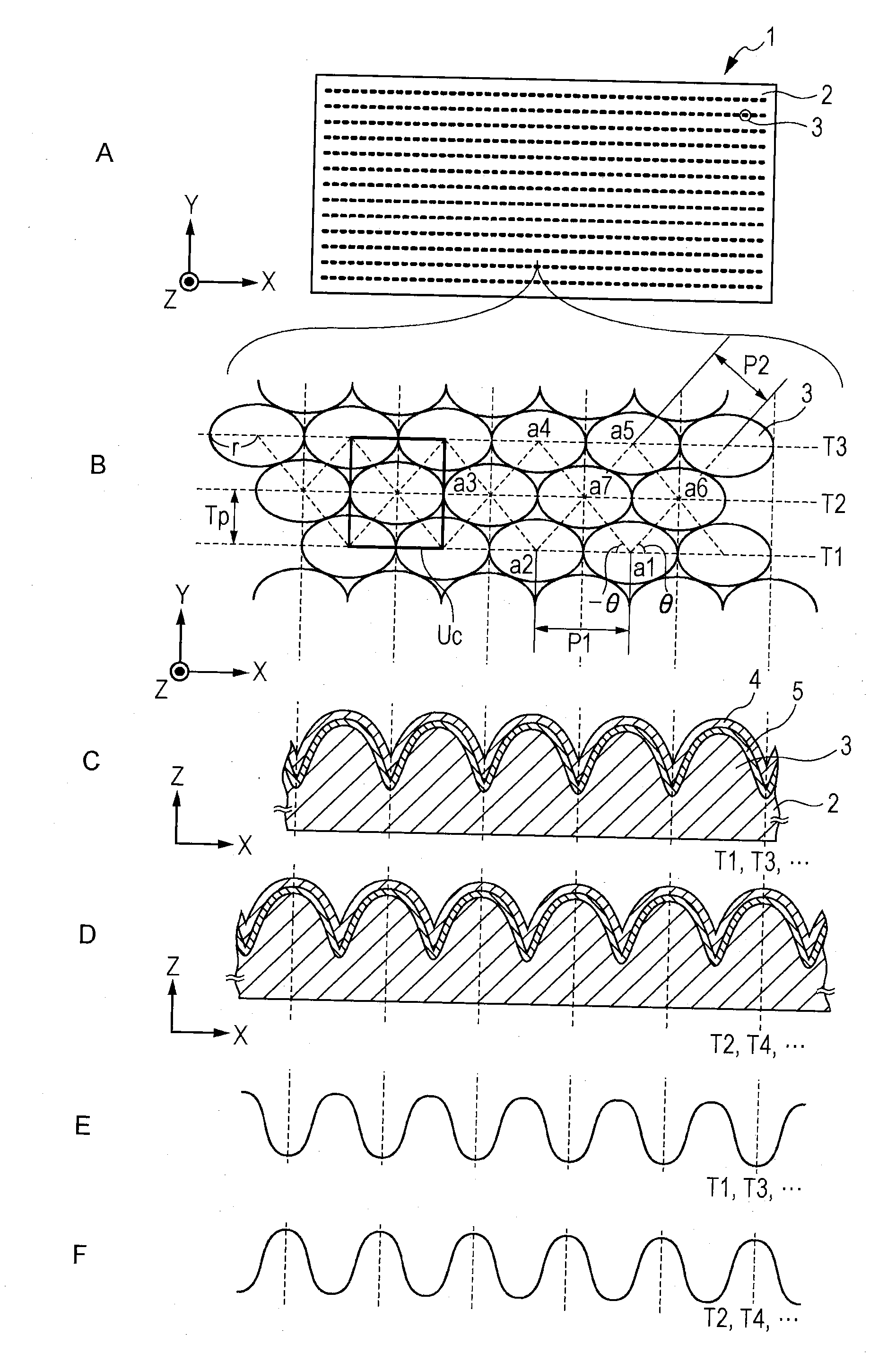
first embodiment (example of two-dimensional arrangement of structures into the shape of a straight line and , in addition , the shape of a hexagonal lattice : refer to fig.1)
1. First embodiment (example of two-dimensional arrangement of structures into the shape of a straight line and, in addition, the shape of a hexagonal lattice: refer to FIG. 1)
second embodiment (example of two-dimensional arrangement of structures into the shape of a straight line and , in addition , the shape of a tetragonal lattice : refer to fig.15)
2. Second embodiment (example of two-dimensional arrangement of structures into the shape of a straight line and, in addition, the shape of a tetragonal lattice: refer to FIG. 15)
third embodiment (example of two-dimensional arrangement of structures into the shape of an arc and , in addition , the shape of a hexagonal lattice : refer to fig.18)
3. Third embodiment (example of two-dimensional arrangement of structures into the shape of an arc and, in addition, the shape of a hexagonal lattice: refer to FIG. 18)
Login to View More PUM
| Property | Measurement | Unit |
|---|---|---|
| Thickness | aaaaa | aaaaa |
| Thickness | aaaaa | aaaaa |
| Electrical resistance | aaaaa | aaaaa |
Abstract
An electrically conductive optical element is provided with a substrate having a surface, structures which are convex portions or concave portions in the shape of a cone and which are arranged in large numbers on the surface of the substrate with a minute pitch less than or equal to the wavelength of the visible light, and a transparent, electrically conductive layer disposed on the structures. The aspect ratio of the structure is 0.2 or more, and 1.3 or less, the transparent, electrically conductive layer has a surface following the structures, the average layer thickness Dm1 of the transparent, electrically conductive layer at the top portion of the structure is 80 nm or less, and the surface resistance of the transparent, electrically conductive layer is within the range of 50Ω / □ or more, and 500Ω / □ or less.
Description
TECHNICAL FIELD[0001]The present invention relates to an electrically conductive optical element, a touch panel, an information input device, a display device, a solar cell, and a stamper for producing an electrically conductive optical element. In particular, it relates to an electrically conductive optical element provided with a transparent, electrically conductive film on one principal surface of a substrate.BACKGROUND ART[0002]In recent years, resistive touch panels to input information have become disposed on display devices, e.g., liquid crystal display element, included in mobile apparatuses and cellular phone apparatuses.[0003]The resistive touch panel has a structure in which two transparent, electrically conductive films are disposed oppositely with a spacer formed from an insulating material, e.g., an acrylic resin, therebetween. The transparent, electrically conductive film functions as an electrode for the touch panel and includes a base member, e.g., a polymer film, h...
Claims
Login to View More Application Information
Patent Timeline
 IPC IPC(8): H02G3/00H01L31/0224B29C59/02
CPCB32B3/30G02B1/11G02B5/0231Y02E10/50G06F3/0428H01L31/022466H01L31/0236G06F3/042H01L31/022475G06F3/045H01B5/14
InventorKAJIYA, SHUNICHITAKENOUCHI, MASAKIENDOH, SOHMEIHAYASHIBE, KAZUYAKIMURA, KIYOHIROMURAMOTO, YUTAKA
OwnerDEXERIALS CORP