Double-layer passivating method for crystalline silicon solar battery

A technology of solar cells and crystalline silicon, applied in coatings, circuits, electrical components, etc., can solve the problems of difficult to obtain high-efficiency cells, high surface recombination speed, low front surface reflection, etc., achieve good anti-reflection performance, low cost, Enhance the effect of internal back reflection

Inactive Publication Date: 2011-05-18
ALTUSVIA ENERGY TAICANG
View PDF4 Cites 28 Cited by
  • Summary
  • Abstract
  • Description
  • Claims
  • Application Information

AI Technical Summary

Problems solved by technology

[0005] The purpose of the present invention is to solve the problem that the surface recombination speed is relatively high after the passivation of the prior art mentioned above, and it is difficult to obtain a high-efficiency battery. And the double-layer passivation method of Al2O3 and SiNx laminates grown by PDV (Physical Vapor Deposition), this method can effectively reduce surface recombination, and can obtain lower front surface reflection and better light trapping effect, which is beneficial to manufacturing High Efficiency Solar Cells

Method used


Image

  • Double-layer passivating method for crystalline silicon solar battery
  • Double-layer passivating method for crystalline silicon solar battery

Examples


Embodiment 1

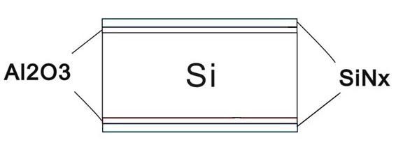
[0021] A double-layer passivation method for crystalline silicon solar cells, the method comprising the following steps:

[0022] (1) Select 10pcs of P-type FZ monocrystalline silicon wafers (1W cm), clean with 1% HF solution, and polish with 20% NaOH solution;

[0023] (2) Use the ALD method to grow Al2O3 on the silicon wafer obtained in step (1), with a refractive index of 1.6 and a thickness of 30nm;

[0024] (3) Use the PECVD method to grow SiNx on the silicon wafer obtained in step (2), with a refractive index of 2.05 and a thickness of 100nm;

[0025] (4) Anneal the sample obtained in step (3) at a temperature of 400° C. in an N2 atmosphere for 10 minutes to obtain a double-layer passivation dielectric film.

[0026] Implementation Effect:

[0027] The passivation effect of the double-layer passivation dielectric film manufactured by the method described in Example 1 is excellent, and the surface recombination speed reaches 3 cm / s, which is far superior to the current ...

Embodiment 2

[0029] A double-layer passivation method for crystalline silicon solar cells, the method comprising the following steps:

[0030] (1) Select 10pcs (1W cm) of N-type FZ single crystal silicon wafers, use 1% HF solution for cleaning, use 2.5% NaOH solution for texturing, and use BBr3 diffusion, the square resistance is 50W / sq;

[0031] (2) Use the ALD method to grow Al2O3 on the silicon wafer obtained in step (1), with a refractive index of 1.65 and a thickness of 15nm;

[0032] (3) Use the PECVD method to grow SiNx on the silicon wafer obtained in step (2), with a refractive index of 2.05 and a thickness of 70nm;

[0033] (4) Anneal the sample obtained in step (3) at a temperature of 400° C. in an N2 atmosphere for 10 minutes to obtain a double-layer passivation dielectric film.

[0034] Implementation Effect:

[0035] The double-layer passivation dielectric film manufactured by the method described in Example 2 has an excellent passivation effect, and the surface recombinati...

Embodiment 3

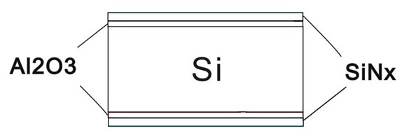
[0037] A double-layer passivation method for crystalline silicon solar cells, the method comprising the following steps:

[0038] (1) Select 10pcs of P-type FZ monocrystalline silicon wafers (1W cm), clean with 1% HF solution, and polish with 20% NaOH solution;

[0039] (2) Use the PECVD method to grow Al2O3 on the silicon wafer obtained in step (1), with a refractive index of 1.6 and a thickness of 15nm;

[0040] (3) Use the PVD method to grow SiNx on the silicon wafer obtained in step (2), with a refractive index of 2.15 and a thickness of 80nm;

[0041] (4) Annealing the sample obtained in step (3) at a temperature of 450° C. in an N2 atmosphere for 6 minutes to obtain a double-layer passivation dielectric film.

[0042] Implementation Effect:

[0043] The passivation effect of the double-layer passivation dielectric film manufactured by the method described in Example 3 is excellent, and the surface recombination speed reaches 5 cm / s, which is far superior to the current...


PUM

PropertyMeasurementUnit
thicknessaaaaaaaaaa
thicknessaaaaaaaaaa
thicknessaaaaaaaaaa

Abstract

The invention discloses a double-layer passivating method for a crystalline silicon solar battery, comprising the following steps: (1) selecting a silicon chip, cleaning, and polishing or texturing; (2) growing Al2O3 on the silicon chip obtained in step (1) by an ALD (atomic layer deposition) or PECVD (plasma enhanced chemical vapor deposition) method, wherein the refractive index is 1.5-1.7, the thickness is 10-80nm; (3) growing SiNx on the silicon chip obtained in step (2) by the PECVD or PVD (physical vapor deposition) method, wherein the refractive index is 1.9-2.2, the thickness is 30-150nm; and (4) annealing the sample obtained in step (3) at the temperature of 200-600 DEG C in the atmosphere of N2 or a hydrogen argon gas mixture for 1-30 minutes to obtain a double-layer passivated dielectric film. The passivating method provided by the invention can reduce the surface recombination velocity of the silicon chip to below 10cm/s, can be well applied to surface passivation of a crystalline silicon solar battery, and obtains high conversion efficiency.

Description

technical field [0001] The invention relates to the field of photovoltaic applications, in particular to a double-layer passivation method for crystalline silicon solar cells. Background technique [0002] So far, the photovoltaic market is mainly flooded with two products, one is crystalline silicon solar cells, and the other is thin-film solar cells. Crystalline silicon solar cells have always occupied the mainstream position, and crystalline silicon solar cells will still be the mainstream in the next few years or even decades. In order to increase the cost competitiveness of crystalline silicon solar cells, it is necessary to increase the conversion efficiency of the cell or reduce the thickness of the silicon wafer. Both high-efficiency cells and reduced silicon wafer thickness are affected by the surface recombination rate (SRV). With the thinning of the silicon wafer, the passivation of the front and rear surfaces of the high-efficiency battery, and the internal ref...

Claims


Application Information

Patent Timeline
Patent Type & Authority Applications(China)
IPC IPC(8): H01L31/18C23C16/40C23C16/34C23C14/06
CPCY02P70/50
Inventor 夏正月李晓强陶龙忠
Owner ALTUSVIA ENERGY TAICANG
Why Eureka
Try Eureka