Semiconductor device

a semiconductor device and channel mobility technology, applied in the direction of semiconductor devices, basic electric elements, electrical appliances, etc., can solve the problems of reducing the manufacturing cost of semiconductor devices and achieving both sufficient channel mobility, and achieve the effect of reducing manufacturing costs and sufficient channel mobility

Inactive Publication Date: 2012-07-12
SUMITOMO ELECTRIC IND LTD
View PDF7 Cites 7 Cited by
  • Summary
  • Abstract
  • Description
  • Claims
  • Application Information

AI Technical Summary

Benefits of technology

[0007]The present invention is made in view of the foregoing problem, and has its object to provide a method for

Problems solved by technology

In such a semiconductor device, it is difficult to achieve both sufficient channel mo

Method used


Image

  • Semiconductor device
  • Semiconductor device
  • Semiconductor device

Examples


first embodiment

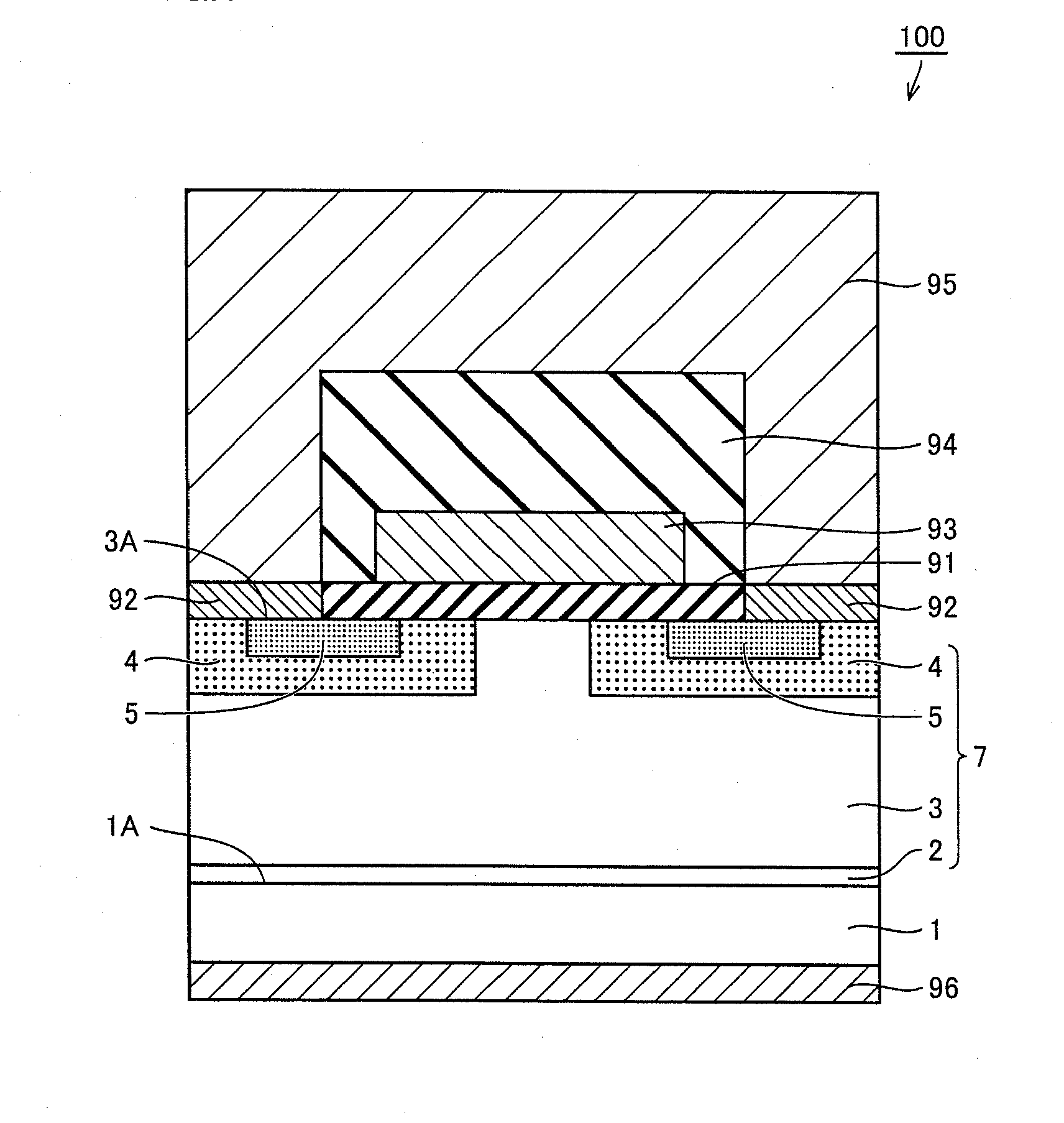
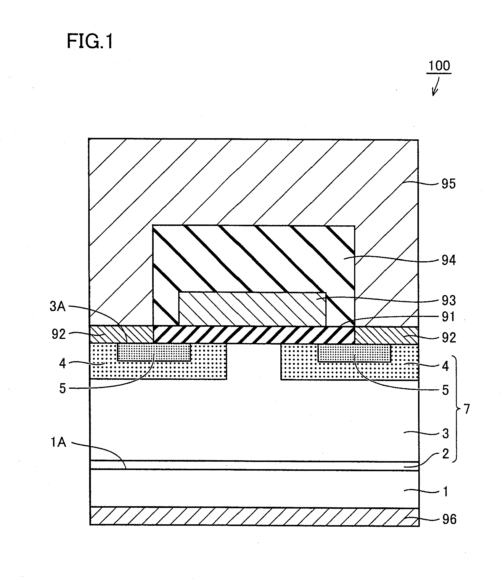
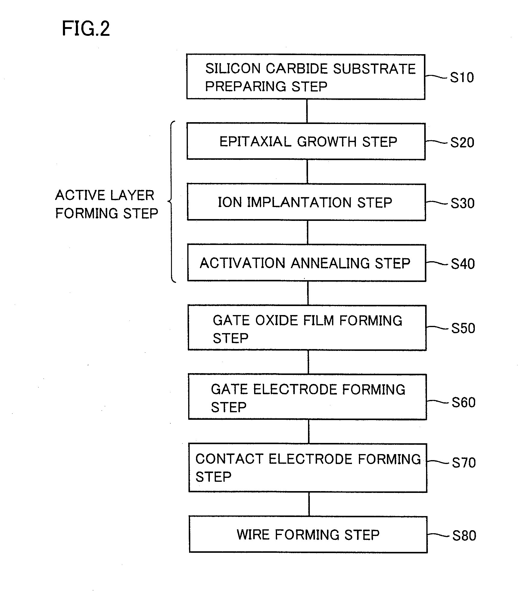
[0046]First, a first embodiment, which is one embodiment of the present invention, will be described. Referring to FIG. 1, a MOSFET 100, which is a semiconductor device in the present embodiment, includes: a silicon carbide substrate 1 having n type conductivity; a buffer layer 2 made of silicon carbide and having n type conductivity; a drift layer 3 made of silicon carbide and having n type conductivity; a pair of p type body regions 4 each having p type conductivity; and n+ regions 5 each having n type conductivity.

[0047]Buffer layer 2 is formed on one main surface 1A of silicon carbide substrate 1, and contains an n type impurity and therefore has n type conductivity. Drift layer 3 is formed on buffer layer 2, and contains an n type impurity and therefore has n type conductivity. The n type impurity contained in drift layer 3 is, for example, N (nitrogen), and is contained therein at a concentration (density) lower than that of the n type impurity contained in buffer layer 2. Buf...

second embodiment

[0081]The following describes another embodiment of the present invention, i.e., a second embodiment. An IGBT 200, which is a semiconductor device of the second embodiment, has a structure similar to that of MOSFET 100 in the first embodiment, in terms of the plane orientation of the silicon carbide substrate, the p type impurity density of the p type body region, and the omission of the p+ region in the first embodiment. Hence, IGBT 200 provides an effect similar thereto.

[0082]Specifically, referring to FIG. 8, IGBT 200, which is a semiconductor device in the present embodiment, includes: a silicon carbide substrate 201 having p type conductivity; a buffer layer 202 (which may have n type or p type conductivity); a drift layer 203 made of silicon carbide and having n type conductivity; and a pair of p type body regions 204 each having p type conductivity; and n+ regions 205 each having n type conductivity.

[0083]Buffer layer 202 is formed on one main surface 201A of silicon carbide ...


PUM


Abstract

A MOSFET includes: a silicon carbide substrate having a main surface having an off angle of not less than 50° and not more than 65° relative to a {0001} plane; an active layer; a gate oxide film; a p type body region having p type conductivity and formed to include a region of the active layer, the region being in contact with the gate oxide film; an n+ region having n type conductivity and formed in the p type body region to include a main surface of the active layer opposite to the silicon carbide substrate; and a source contact electrode formed on the active layer in contact with the n+ region, the p type body region having a p type impurity density of 5×1017 cm−3 or greater, the source contact electrode and the p type body region being in direct contact with each other.

Description

BACKGROUND OF THE INVENTION[0001]1. Field of the Invention[0002]The present invention relates to a semiconductor device, more particularly, a semiconductor device achieving both sufficient channel mobility and reduced manufacturing cost of the semiconductor device.[0003]2. Description of the Background Art[0004]In recent years, in order to achieve high breakdown voltage, low loss, and utilization of semiconductor devices under a high temperature environment, silicon carbide has begun to be adopted as a material for a semiconductor device. Silicon carbide is a wide band gap semiconductor having a band gap larger than that of silicon, which has been conventionally widely used as a material for semiconductor devices. Hence, by adopting silicon carbide as a material for a semiconductor device, the semiconductor device can have a high breakdown voltage, reduced on-resistance, and the like. Further, the semiconductor device thus adopting silicon carbide as its material has characteristics...

Claims


Application Information

Patent Timeline
IPC IPC(8): H01L29/161
CPCH01L21/047H01L29/045H01L29/7395H01L29/66068H01L29/1608
Inventor HIYOSHI, TORUTAMASO, HIDETO
Owner SUMITOMO ELECTRIC IND LTD
Why Eureka
Try Eureka