
Self-Aligned Multi-Dielectric-Layer Lift Off Process for Laser Diode Stripes

a laser diode strip and dielectric layer technology, applied in the field of optical devices, can solve the problems of conventional edison light bulbs, light bulbs dissipate much thermal energy, conventional light bulbs routinely fail,

Active Publication Date: 2012-07-12
KYOCERA SLD LASER INC
View PDF4 Cites 191 Cited by
  • Summary
  • Abstract
  • Description
  • Claims
  • Application Information

AI Technical Summary

Benefits of technology

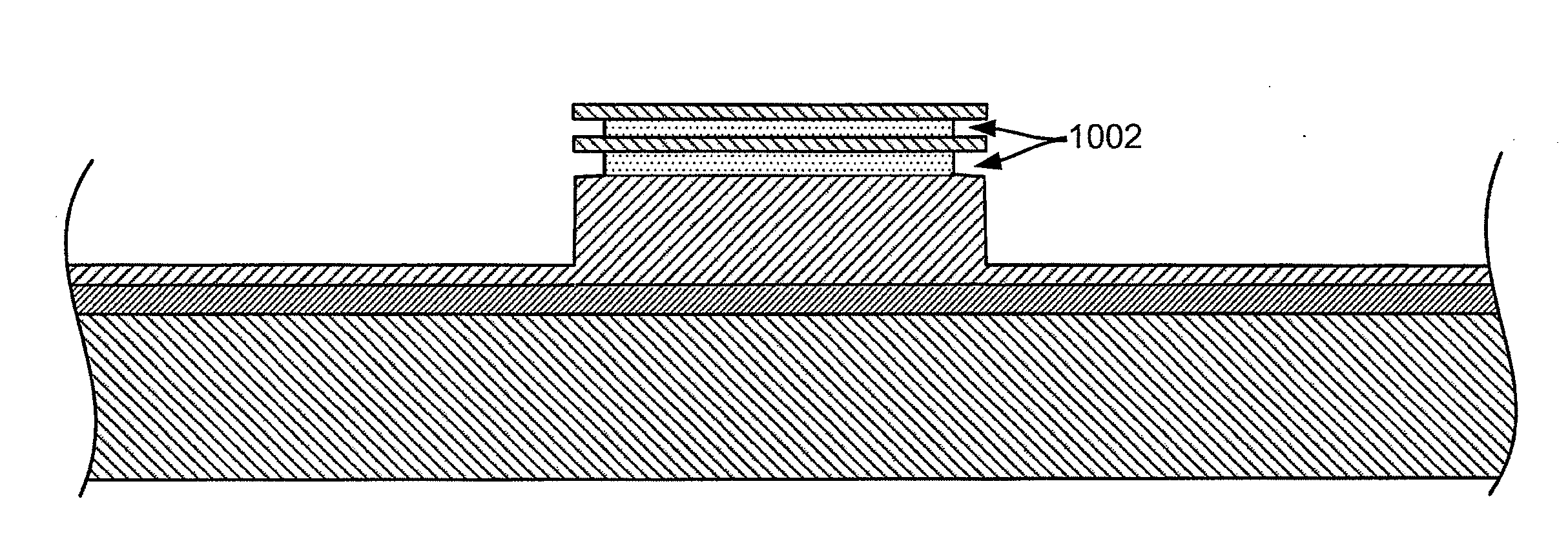
[0011]Many benefits can be achieved by ways of the present invention. For example, the multilayer mask structure eliminates the use of a photoresist material to expose a top surface region. The top surface region allows for a contact structure to form for the optical device structure according to one or more embodiments. In addition, the multilayer mask structure also provides for a thick dielectric mask without incurring stress on the optical device structure according to one or more embodiments. Depending on the embodiment, one or more of these benefits can be achieved. Further detail of the method and the benefits can be found throughout the present specification and particularly below.

Problems solved by technology

Unfortunately, drawbacks exist with the conventional Edison light bulb.
That is, the conventional light bulb dissipates much thermal energy leading to inefficiencies.
Additionally, the conventional light bulb routinely fails often due to thermal expansion and contraction of the filament element.
High intensity green LEDs based on GaN have been proposed and even demonstrated with limited success.
Unfortunately, achieving high intensity, high-efficiency GaN-based green LEDs has been problematic.
The performance of optolectronic devices fabricated on conventional c-plane GaN suffer from strong internal polarization fields, which leads to poor radiative recombination efficiency.
Since this phenomenon becomes more pronounced in InGaN layers with increased indium content for increased wavelength emission, extending the performance of GaN-based LEDs to the green regime has been difficult.
Furthermore, increased indium content in a GaN film often requires reduced growth temperature leading to poorer crystal quality of high-indium-content InGaN films.
The difficulty of achieving a high intensity green LED has lead scientists and engineers to the term “green gap” to describe the generally unavailability of such green LED.

Method used


Image

  • Self-Aligned Multi-Dielectric-Layer Lift Off Process for Laser Diode Stripes
  • Self-Aligned Multi-Dielectric-Layer Lift Off Process for Laser Diode Stripes
  • Self-Aligned Multi-Dielectric-Layer Lift Off Process for Laser Diode Stripes

Examples


Embodiment Construction

[0015]The present invention is directed to optical devices and related methods. More particularly, the present invention provides a method and device for emitting electromagnetic radiation for optical devices using non-polar or semipolar gallium containing substrates such as GaN, AN, InN, InGaN, AlGaN, and AlInGaN, and others. Merely by way of example, the invention can be applied to optical devices, lasers, light emitting diodes (e.g., red, green, blue), solar cells, photoelectrochemical water splitting and hydrogen generation, photodetectors, integrated circuits, and transistors, among other devices.

[0016]As used herein, the term gallium nitride substrate material is associated with Group III-nitride based materials including GaN, InGaN, AlGaN, or other Group III containing alloys or compositions that are used as starting materials. Such starting materials include polar GaN substrates (i.e., substrate where the largest area surface is nominally an (h k 1) plane wherein h=k=0, and ...


PUM


Abstract

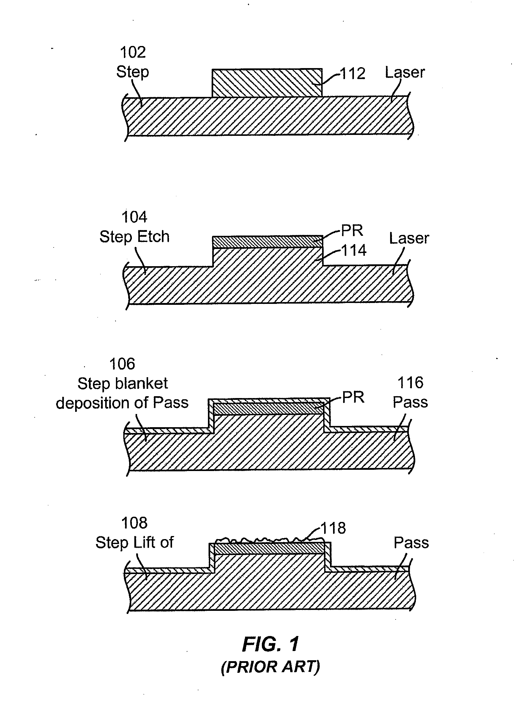
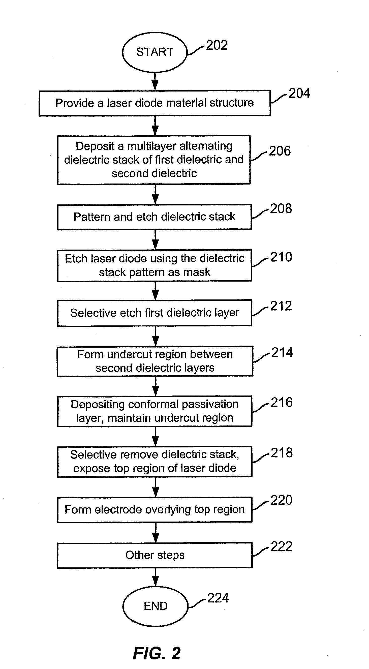
A method for forming a laser diode structure. The method includes providing a laser diode material having a surface region. A multilayer dielectric mask structure comprising alternating first and second dielectric layers is formed overlying the surface region. The method forms a laser diode structure using the multilayer dielectric mask structure as a mask. The method selectively removes a portion of the first dielectric layer to form one or more undercut regions between the second dielectric layers. A passivation layer overlies the multilayer dielectric mask structure and the undercut region remained intact. The dielectric mask structure is selectively removed, exposing a top surface region of the laser diode structure. A contact structure is formed overlying at least the exposed top surface region.

Description

CROSS-REFERENCE TO RELATED APPLICATIONS[0001]This application is a continuation of U.S. application Ser. No. 12 / 502,382, filed Jul. 14, 2009; which application claims priority to U.S. Provisional Application No. 61 / 080,654, filed Jul. 14, 2008, which are incorporated herein by reference for all purposes.BACKGROUND OF THE INVENTION[0002]The present invention is directed to optical devices and related methods. More particularly, the present invention provides a method and device for emitting electromagnetic radiation for optical devices using non-polar or semipolar gallium containing substrates such as GaN, AN, InN, InGaN, AlGaN, and AlInGaN, and others. Merely by way of example, the invention can be applied to optical devices, lasers, light emitting diodes, solar cells, photoelectrochemical water splitting and hydrogen generation, photodetectors, integrated circuits, and transistors, among other devices.[0003]In the late 1800's, Thomas Edison invented the lightbulb. The conventional ...

Claims


Application Information

Patent Timeline
Patent Type & Authority Applications(United States)
IPC IPC(8): H01L33/32
CPCH01S5/34333H01S5/2086H01S2301/176B82Y20/00Y10S438/981Y10S438/951H01S2304/04
Inventor RARING, JAMES W.FEEZELL, DANIEL F.PFISTER, NICK
Owner KYOCERA SLD LASER INC
Learn More