Transparent conductive film and touch panel

a technology of transparent conductive film and touch panel, which is applied in the direction of insulated conductors, cables, instruments, etc., can solve the problems of difficult use in some applications, poor appearance of display devices produced therewith, and low flexibility or workability, and achieve the effect of reducing the amount of conductive film

a technology of transparent conductive film and touch panel, which is applied in the direction of insulated conductors, cables, instruments, etc., can solve the problems of difficult use in some applications, poor appearance of display devices produced therewith, and low flexibility or workability, and achieve the effect of reducing the amount of conductive film

US20120181063A1Inactive Publication Date: 2012-07-19NITTO DENKO CORP

Image

  • Transparent conductive film and touch panel
  • Transparent conductive film and touch panel
  • Transparent conductive film and touch panel

Examples


example 1

(Formation of First Transparent Dielectric Layer)

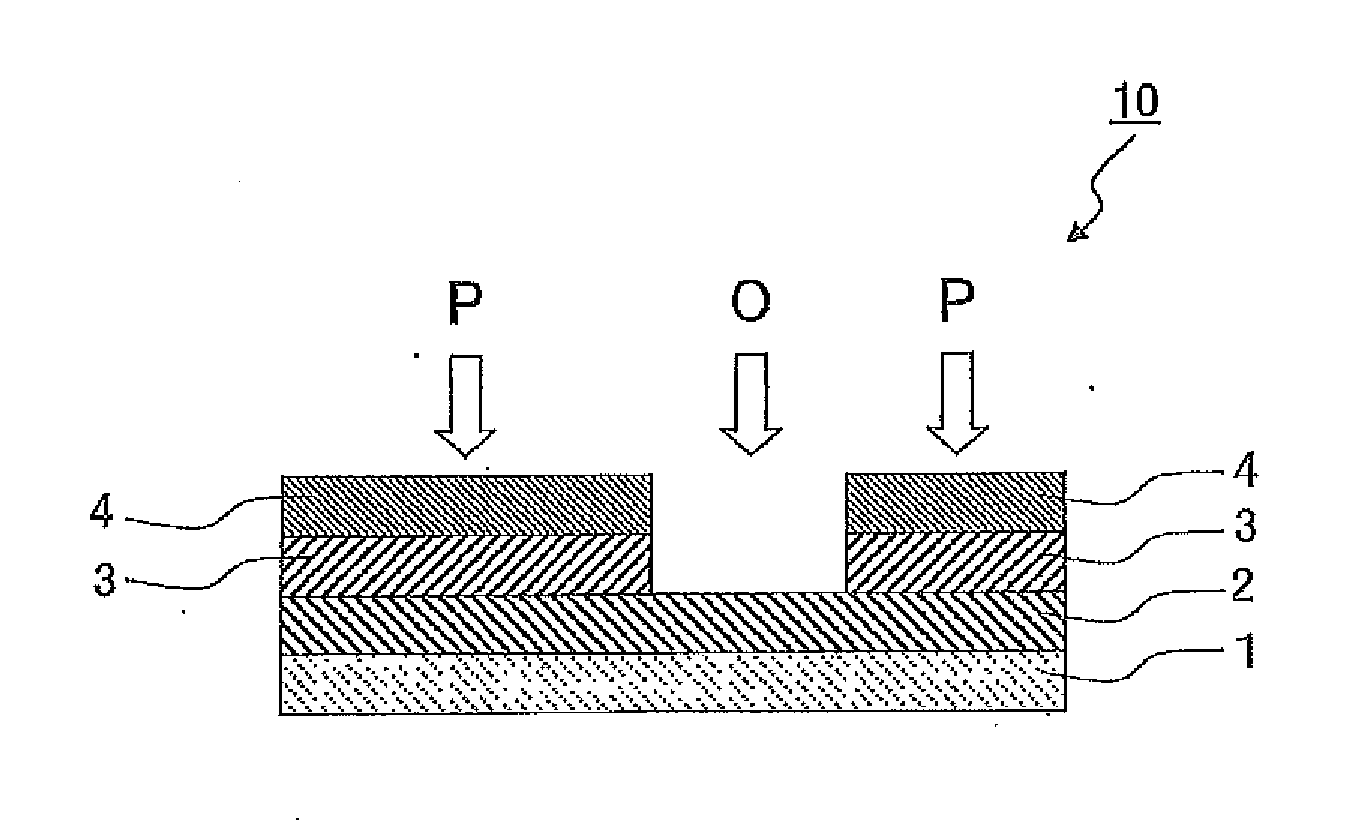
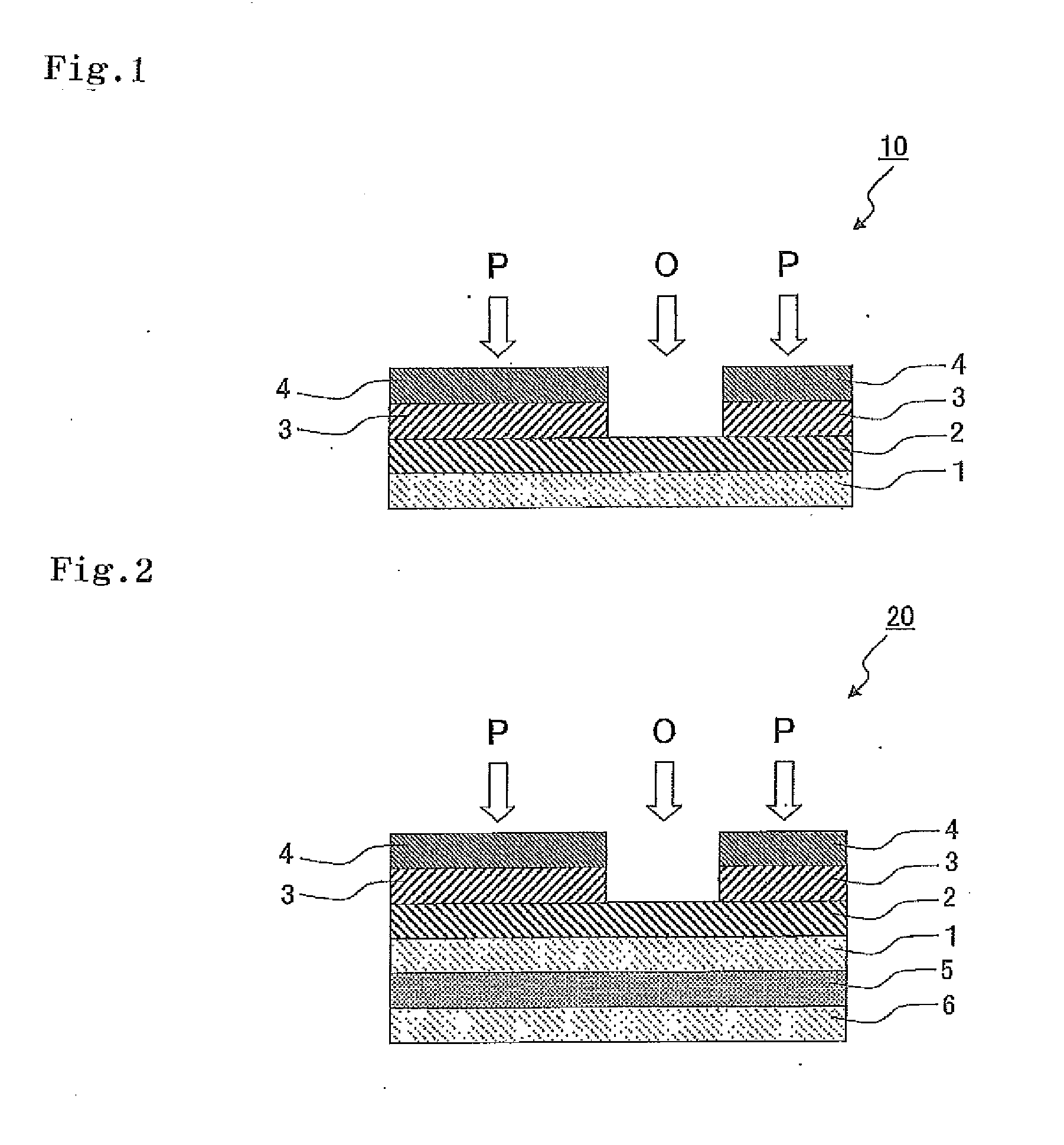
[0063]A first transparent dielectric layer (refractive index n0=1.54, thickness: 4 nm) was formed by applying a thermosetting type resin of a melamine resin:an alkyd resin:an organosilane condensate (weight ratio of 2:2:1) on one surface of a transparent base material (refractive index nf=1.66) consisting of a polyethylene terephthalate film (hereinafter, referred to as a PET film) having a thickness of 125 μm and by curing it.

(Formation of Second Transparent Dielectric Layer)

[0064]A second transparent dielectric layer having a thickness of 20 nm was then formed by performing vacuum deposition of SiO2 (refractive index n1=1.46) on the first transparent dielectric layer with an electron beam heating method at a degree of vacuum of 1×10⁻² to 3×10⁻² Pa.

(Formation of Transparent Conductive Layer)

[0065]An ITO layer (refractive index n2=2.00) having a thickness of 22 nm was then formed, as the transparent conductive layer, on the second tra...

examples 2 to 6

[0068]Transparent conductive films were obtained by performing the same operation as Example 1 except that the thicknesses of the first transparent dielectric layer and the second transparent dielectric layer in Example 1 were adjusted to values shown in Table 1.

example 7

[0069]A transparent conductive film was obtained by performing the same operation as Example 1 except that the first transparent dielectric layer in Example 1 was formed with the method shown below and the thickness of the transparent conductive layer (ITO layer) was 40 nm.

(Method for Forming First Transparent Dielectric Layer in Example 7)

[0070]A first transparent dielectric layer (refractive index n0=2.35, thickness: 8 nm) consisting of titanium oxide was formed on one surface of the transparent base material (refractive index nf=1.66) consisting of a PET film having a thickness of 125 μm with a reactive sputtering method using a titanium target under an atmosphere of a mixed gas (0.5 Pa) of 50% of argon gas and 50% of oxygen gas.


PUM

PropertyMeasurementUnit
Thicknessaaaaaaaaaa
Thicknessaaaaaaaaaa
Thicknessaaaaaaaaaa

Abstract

The present invention relates to a transparent conductive film in which a transparent conductive layer is patterned and that is capable of suppressing deterioration of the appearance due to the difference in hues of reflected light between the pattern portion and the portion directly under the pattern opening portion, and a touch panel that uses it. In the transparent conductive film (10) of the present invention, a first transparent dielectric layer (2) and a transparent conductive layer (4) are formed on a transparent base material (1) in this order. It is preferable that a relationship 0≦|a*P−a*O|≦4.00 is satisfied and a relationship 0≦|b*P−b*O|≦5.00 is satisfied where a hue a* value and a hue b* value of reflected light when the pattern portion (P) is irradiated with white light are a*P and b*P, respectively, and a hue a* value and a hue b* value of reflected light when a portion directly under the pattern opening portion (O) is irradiated with white light are a*O and b*O, respectively.

Description

TECHNICAL FIELD[0001]The present invention relates to a transparent conductive film and a touch panel that uses it.BACKGROUND ART[0002]A transparent conductive member that is transparent in the visible light region and that has conductivity has been used for preventing static charge, shielding an electromagnetic wave, etc. in articles in addition to being used as a transparent electrode in displays such as a liquid crystal display and an electroluminescent display, and touch panels.[0003]Concerning conventional transparent conductive components, the so-called conductive glass is well known, which includes a glass member and an indium oxide thin film formed thereon. Since the base material of the conductive glass is made of glass, however, it has low flexibility or workability and is difficult to be used in some applications. In recent years, therefore, transparent conductive films using various types of plastic films such as polyethylene terephthalate films as their substrates have ...

Claims


Application Information

Patent Timeline
19 Jul 2012
Publication
US20120181063A1
IPC
H01B7/02
CPC
G06F3/045; G06F3/044; G06F2203/04103; G06F3/0443; B32B7/02; H01B5/14; H01B13/00
Inventors
NAKAJIMA, KAZUHIRO; SUGAWARA, HIDEO