Power synthesis circuit for radio frequency power amplifier

a power amplifier and power synthesis technology, applied in amplifier combinations, amplifier combinations, multiple-port networks, etc., can solve the problems of not only complicated circuit design, but also impose tough requirements on the circuit components of the rf power amplifier power combiner, so as to improve the reliability of the whole radio frequency combiner network, improve the connection and reduce the voltage swing of the cmos switch

Inactive Publication Date: 2012-07-19
ZYW MICROELECTRONICS
View PDF0 Cites 9 Cited by
  • Summary
  • Abstract
  • Description
  • Claims
  • Application Information

AI Technical Summary

Benefits of technology

[0004]The present invention aims at solving the problems of low integration, high cost and the complexity of the RF switch control circuit in traditional RF power amplifier combiner circuits using GaAs technology switches, thereby providing a novel RF power combining method and its combiner circuit with a CMOS technology switch.
[0009]The switching elements of the circuit in this invention can all be realized with common CMOS technology. Considering the relatively low breakdown voltage of CMOS technology switches, reasonable measures have been taken to improve the CMOS switch connection in the power combination network so as to reduce the voltage swing on the CMOS switches as much as possible in order to increase the reliability of the whole radio frequency combiner network; and by flexibly controlling the connection and disconnection of the switches in the whole power combination network, the combination of matching networks under different working patterns is realized and signal leakage between different channels is avoided, thus the transmitting quality of the radio frequency signal is guaranteed and the performance of the whole wireless communication system is effectively strengthened.
[0010]Compared with the RF power amplifier power combiner circuit with a PHEMT switch currently made with expensive GaAs technology, the present invention also has the advantages of high integration, low cost, and a simple switch control circuit.

Problems solved by technology

Therefore, the performance of RF power amplifier power-combiner circuit in such things as power capacity, insertion loss, isolation, and anti-voltage breakdown ability will greatly affect the performance of the entire wireless communication system.
And these performance indicators also impose tough requirements on the RF power amplifier power combiner circuit components such as switches and duplexers.
To meet the high requirements of the RF power amplifier, expensive GaAs technology is adopted for the design of most power-combiner circuit switches, the disadvantages of which include not only complicated circuit design, but also high cost, low integration and immature process compared to common CMOS technology.
And for the whole RF power amplifier power combiner circuit, its isolation degree will also affect the overall system performance.
Since switch SW1 must bear all of the PA transmit power, it must have a high breakdown voltage and over-power capability, which means only expensive GaAs technology with high breakdown voltage is available to make the switch, and the insertion loss of the switch cascaded in the emission path will directly impact the power of the antenna side; when RX side receives power, the signals at the antenna end reach the receiver through the duplexer and SW5-SW8, and the receiver insertion loss of switch SW5-SW8 cascaded in the receiving path will directly affect receiver sensitivity of the entire communication system.
However, the PHEMT tube is a depletion-mode FET, and drives the gate with negative voltage, which increases design complexity and the cost of design and production of the switch control circuit.
While designing switches with the CMOS technology has the advantages of high integration, technical maturity and low cost, it also has the disadvantes of low breakdown voltage, and a limited switch isolation degree.

Method used


Image

  • Power synthesis circuit for radio frequency power amplifier
  • Power synthesis circuit for radio frequency power amplifier
  • Power synthesis circuit for radio frequency power amplifier

Examples


Embodiment Construction

[0015]Further description of the present invention is given in combination with the drawings and embodiments to facilitate understanding by those skilled in this art.

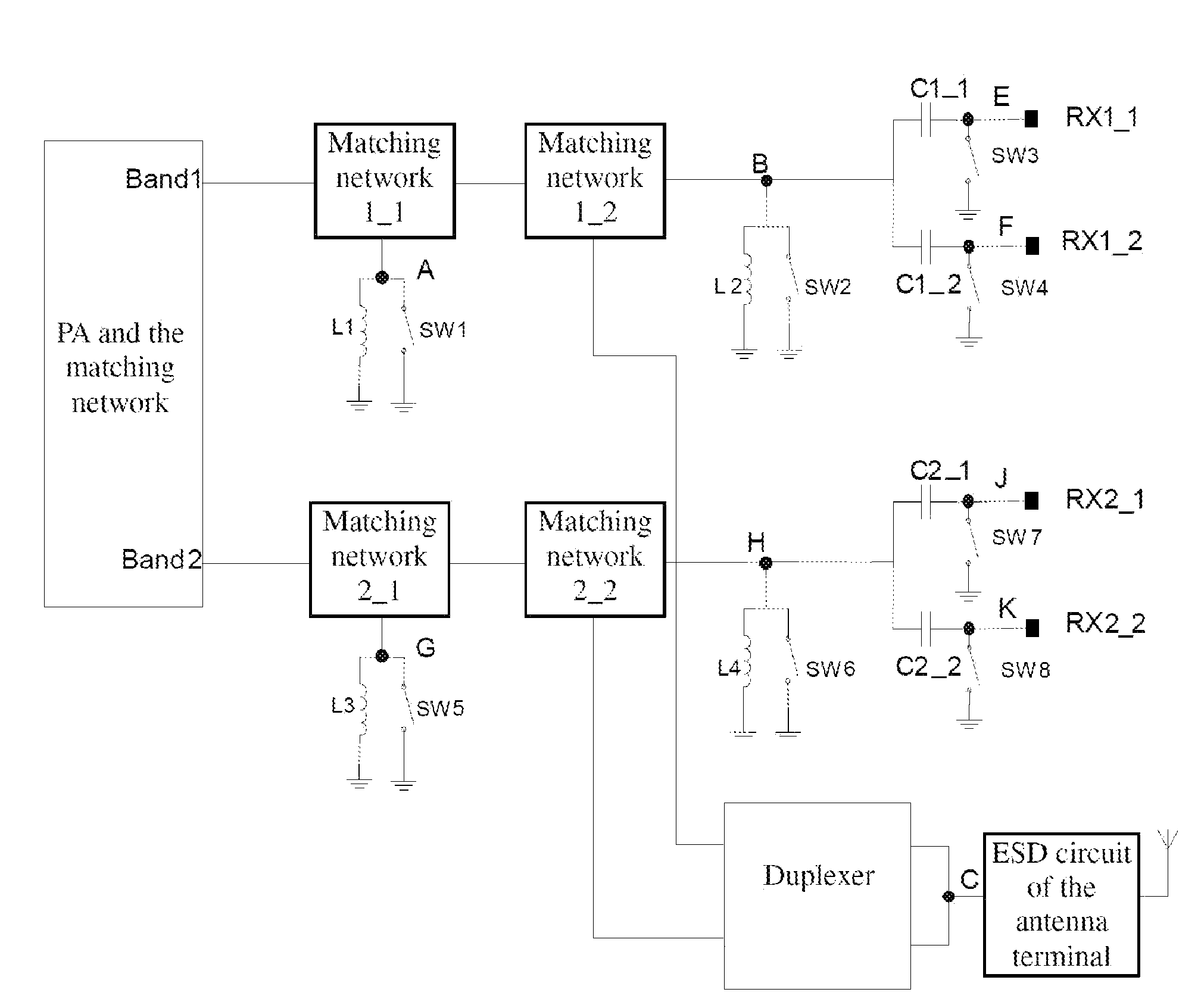
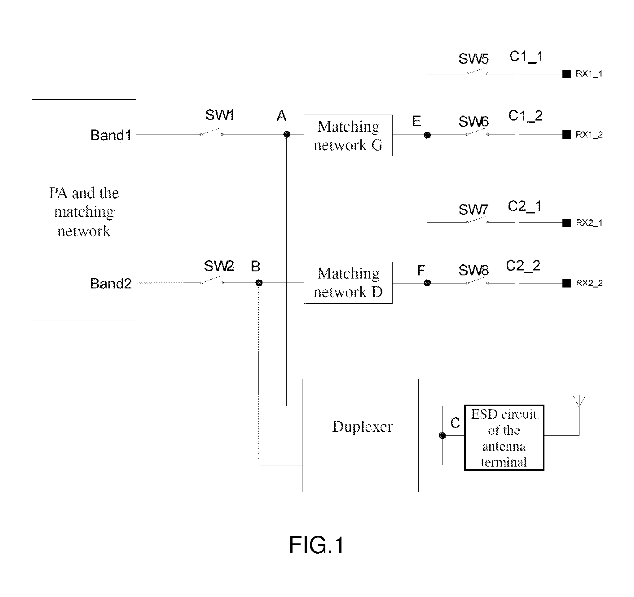
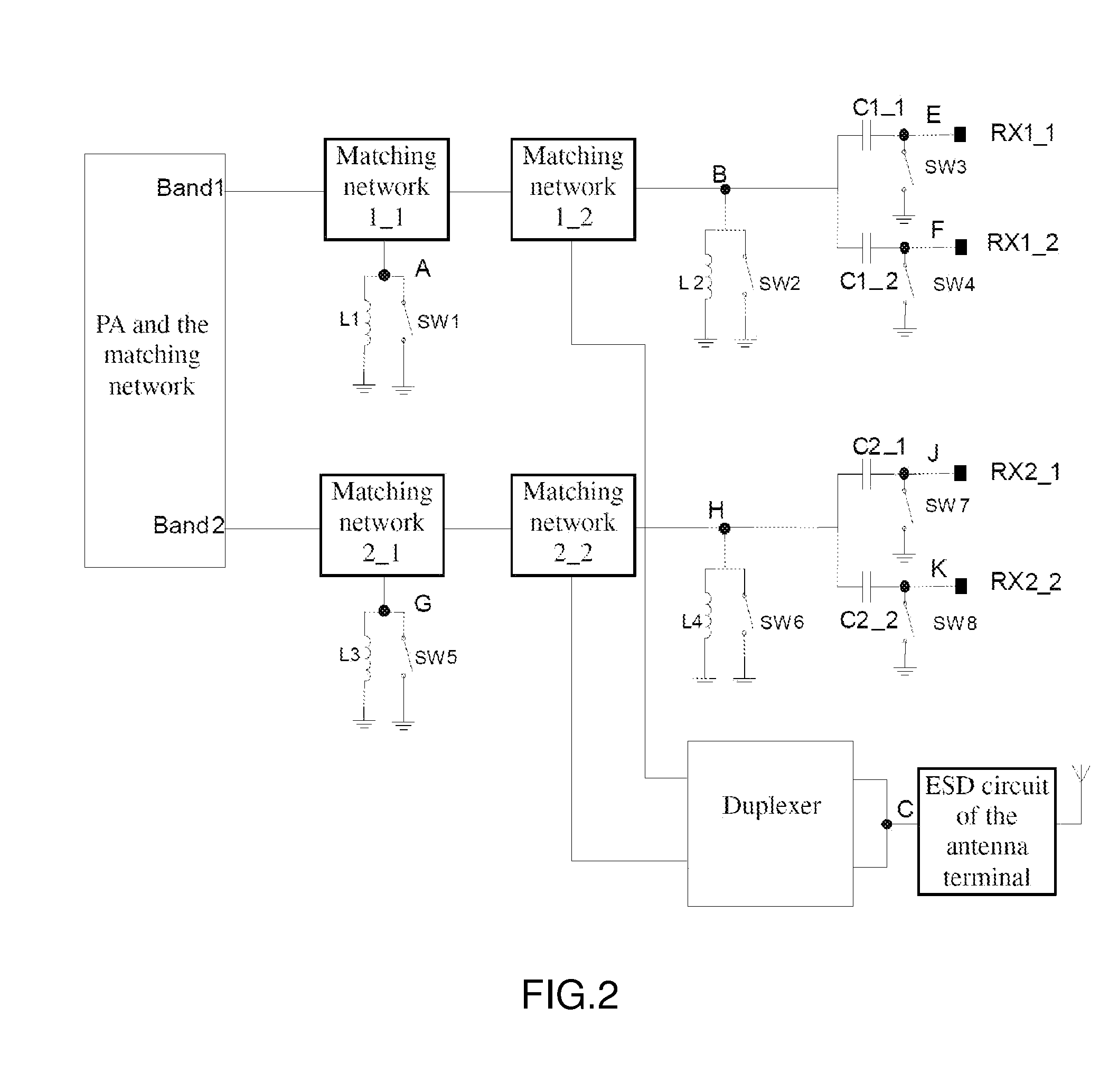
[0016]FIG. 2 shows the first embodiment of RF power combination of the circuit in the present invention with CMOS switches. All of the switches SW1, SW2, SW3, SW4, SW5, SW6, SW7, SW8 are grounded in parallel. Through signal switching by controlling the connection and disconnection of the switches and with the coordination of matching networks 1_1, 1_2, 2_1, 2_2, the voltage swing on the switch is greatly reduced, thus overcoming the defects of low breakdown voltage of the CMOS technology.

[0017]The working principle of the diagram is as follows: when Band1 channel transmits power, the switches SW1, SW2, SW3, SW4, SW6, SW7, SW8 are closed and grounded, and switch SW5 is disconnected. Meanwhile, Node A, node B and node H are directly connected to the ground through the switch, shielding their own parallel inductance. RF si...


PUM


Abstract

A power synthesis circuit for a radio frequency (RF) power amplifier comprises a first matching network and a second matching network, which are connected with two-band signal output ports of the RF power amplifier respectively, and signal coupling circuits which are connected with two-band signal receiving ports respectively. The first matching network and the second matching network are connected with an antenna circuit via a duplexer, and are grounded via an inductor and a switch element which is connected in parallel to the inductor respectively. The leakage of signal among different channels is prevented. The transmission quality of the RF signal is improved. The cost of the power amplifier is reduced and the structure of the power amplifier is simplified.

Description

BACKGROUND OF THE INVENTION[0001]The present invention relates to the field of RF power amplifier technology, specifically to the power combining method and the power-combiner circuit for a RF power amplifier.[0002]The RF power amplifier (PA) is an important part of the wireless communication system. PA, used for the final stage of the transmitter, amplifies the modulated band signal to the required power value and passes it to the antenna for transmission. A communication system often works in multiple frequency bands, which requires a system of multi-channel switches to realize independent working of different bands. However, there is usually only one antenna equipped on the handheld device for the sake of smaller volume and increased portability, so the RF power amplifier power combiner circuit shall control between the RF power amplifier and the antenna. Therefore, the performance of RF power amplifier power-combiner circuit in such things as power capacity, insertion loss, isol...

Claims


Application Information

Patent Timeline
Patent Type & Authority Applications(United States)
IPC IPC(8): H01P5/12H04B1/04H04B1/40H04B1/44
CPCH03F1/565H03F3/24H03F3/68H03F2200/387H03H2007/386H03F1/52H03F2200/111H03F2200/451
Inventor PENG, FENGXIONGZHANG, XUGUANG
Owner ZYW MICROELECTRONICS
Why Eureka
Try Eureka