Template, method for manufacturing the template and method for manufacturing vertical type nitride-based semiconductor light emitting device using the template

a technology of nitride-based semiconductors and templates, which is applied in the direction of polycrystalline material growth, chemically reactive gas growth, crystal growth process, etc., can solve the problems of high manufacturing cost, complex manufacturing process, and severe lattice distortion, so as to reduce stress and prevent dislocation

Inactive Publication Date: 2012-07-26
SEMIMATERIALS +1
View PDF4 Cites 131 Cited by
  • Summary
  • Abstract
  • Description
  • Claims
  • Application Information

AI Technical Summary

Benefits of technology

[0009]An aspect of the present invention is to provide a method for manufacturing a template and a method for manufacturing a nitride-based semiconductor light emitting device using the template, in which a nitride buffer layer having a porous structure is formed on a substrate, thereby reducing stress caused by a difference in lattice constant between the substrate and a nitride layer while preventing dislocation.

Problems solved by technology

However, since a substrate formed of a material such as sapphire (Al2O3) generally has a different lattice constant than a nitride layer, severe lattice distortion occurs when the nitride layer is directly grown on the substrate.
However, since a dislocation density of 109 to 1010 / cm2is obtained even in such a method, there is a limitation in improving crystal quality of the nitride layer.
However, since the growth technique includes SiO2 film deposition based on chemical vapor deposition (CVD), resist coating, photolithography, etching and cleaning, and the like, the manufacturing process is complicated and takes much time.

Method used


Image

  • Template, method for manufacturing the template and method for manufacturing vertical type nitride-based semiconductor light emitting device using the template
  • Template, method for manufacturing the template and method for manufacturing vertical type nitride-based semiconductor light emitting device using the template
  • Template, method for manufacturing the template and method for manufacturing vertical type nitride-based semiconductor light emitting device using the template

Examples


Embodiment Construction

[0020]Exemplary embodiments of the invention will be described in detail with reference to the accompanying drawings. In the following embodiments, a template used in manufacturing a light emitting device will be mainly described. However, the present invention is not limited thereto, but may be applied to various templates used for growth of a nitride layer.

[0021]It will be understood that when an element such as a layer, film, region or substrate is referred to as being “on” another element, it can be directly on the other element or intervening elements may also be present. In contrast, when an element is referred to as being “directly on” another element, there are no intervening elements present.

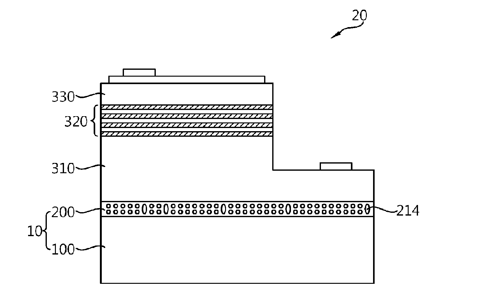
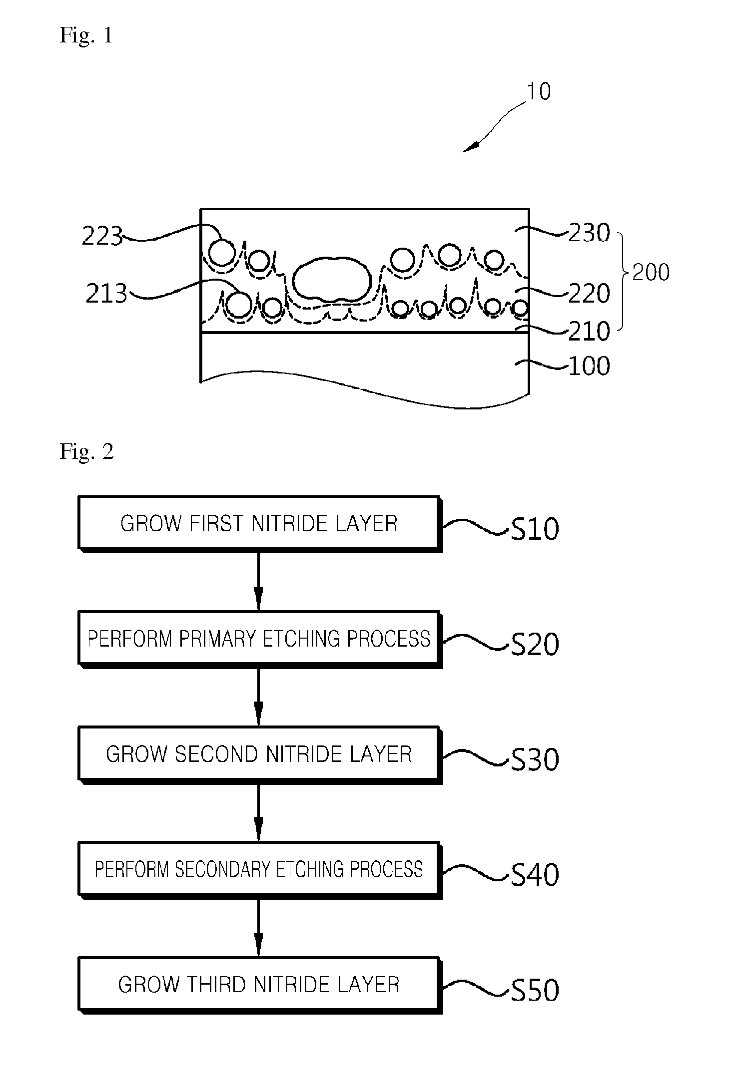
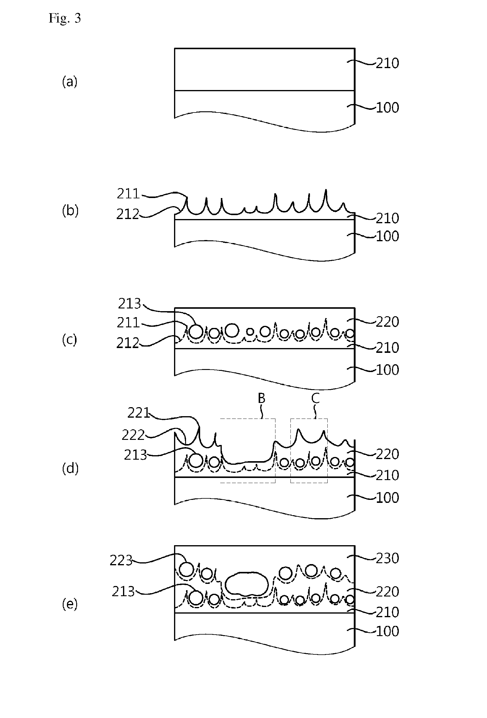
[0022]FIG. 1 is a sectional view of a template 10 according to an exemplary embodiment of the present invention.

[0023]As shown in FIG. 1, the template 10 according to this embodiment includes a substrate 100 and a nitride buffer layer 200 grown on the substrate 100. The nitride buffer l...


PUM

PropertyMeasurementUnit
thicknessaaaaaaaaaa
thicknessaaaaaaaaaa
temperatureaaaaaaaaaa

Abstract

Disclosed herein is a method for manufacturing a template. The method includes growing a first nitride layer on a substrate; etching a top surface of the first nitride layer by supplying a chloride-based etching gas thereto; forming a plurality of first voids by growing a second nitride layer on the top surface of the first nitride layer; etching a top surface of the second nitride layer by supplying the etching gas thereto; and forming a plurality of second voids by growing a third nitride layer on the top surface of the second nitride layer. A method for manufacturing a nitride-based semiconductor light emitting device using the template is also disclosed. As a result, stress between lattices and dislocation defects are reduced by a plurality of voids formed in a nitride buffer layer, thereby improving quality of nitride layers grown in a template. In the case where a light emitting device is manufactured using the template, it is possible to improve workability of the manufacturing process and to enhance luminous efficacy of the light emitting device.

Description

CROSS-REFERENCE TO RELATED APPLICATION[0001]This application claims the benefit under 35 U.S.A. §119 of Korean Patent Application No. 10-2011-0000643, filed on Jan. 4, 2011 in the Korean Intellectual Property Office, the entirety of which is incorporated herein by reference.BACKGROUND[0002]1. Technical Field[0003]The present invention relate to a technique for manufacturing a nitride-based semiconductor light emitting device using a template.[0004]2. Description of the Related Art[0005]Demand for nitride-based semiconductor light emitting devices continues to increase because of various advantages thereof, such as a long lifespan, low power consumption, excellent initial driving characteristics, high vibration resistance, and the like.[0006]In general, a nitride-based semiconductor light emitting device includes a plurality of nitride layers including an n-type nitride layer, an active layer and a p-type nitride layer. Here, the n-type and p-type nitride layers provide electrons and...

Claims


Application Information

Patent Timeline
Patent Type & Authority Applications(United States)
IPC IPC(8): H01L33/62C30B25/02
CPCH01L21/0237H01L21/0242H01L21/02458H01L21/02502H01L21/02513Y10T117/10H01L21/0262H01L21/02656H01L33/007H01L33/025H01L33/22H01L21/0254H01L33/12
Inventor OH, CHUNG-SEOKJANG, SUNG-HWANJUNG, HO-ILPARK, CHI-KWONPARK, KUN
Owner SEMIMATERIALS
Why Eureka
Try Eureka