High-frequency vertical spring probe card structure

a probe card and high-frequency technology, applied in the field of probe card structure, can solve the problems of increasing the cost of the probe, requiring much time and work to assemble each probe, and still having lots of disadvantages, so as to improve the stability of the test, save time and cost, and improve the effect of stability

Inactive Publication Date: 2012-07-26
PLEADER YAMAICHI
View PDF16 Cites 14 Cited by
  • Summary
  • Abstract
  • Description
  • Claims
  • Application Information

AI Technical Summary

Benefits of technology

[0012]1) The high-frequency vertical spring probe card structure can be manufactured by advanced process (e.g. LIGA process, etc.) so as to form multi-layer probe. Compared to conventional machining process, the invention can save much time and cost.
[0013]2) According to the aforesaid advantage, the multi-layer probe manufactured by advanced process has better evenness than the conventional probe, so it can increase testing stability. However, the conventional machining process cannot guarantee that all conventional probes can contact corresponding contact points stably.
[0014]3) The lateral shape of the high-frequency vertical spring probe card structure is flatter than that of the conventional probe, so more probes can be installed on the probe card of the invention. Furthermore, the pitch between two probe tips is also smaller than that of the conventional probe such that the invention can satisfy a great quantity of probes needed by industry.
[0015]4) The high-frequency vertical spring probe card structure further has the insulating layer except the conductive layer. Compared to the conventional probe without insulation, the invention will not generate additional capacitance and inductance, can improve signal strength, and can reduce audio stream. Therefore, the high-frequency vertical spring probe card structure can be applied to high-frequency testing.
[0016]5) The high-frequency vertical spring probe card structure may use two probes to contact one single solder ball and the design of the other end can increase the pitch. The upper contact ends contact different circuit boards so as to achieve effects of withstanding current and withstanding voltage and reduce signal interference. Consequently, the invention can achieve precision measurement and enhance testing current and power range of chip.

Problems solved by technology

However, the aforesaid conventional probe still has lots of disadvantages.
First, it requires much time and work to assemble each probe by labor and the cost increases accordingly.
Furthermore, since the contact end of the aforesaid probe has a column shape, testing stability will be influenced if the evenness of the contact end is bad.
Still further, it is difficult to manufacture and assemble a great quantity of conventional probes due to limitation of the shape and the pitch between two probes cannot be reduced.
Moreover, parts of the aforesaid are exposed without insulation, so it may generate additional capacitance and inductance easily and is not suitable for high-frequency testing.

Method used


Image

  • High-frequency vertical spring probe card structure
  • High-frequency vertical spring probe card structure
  • High-frequency vertical spring probe card structure

Examples


Embodiment Construction

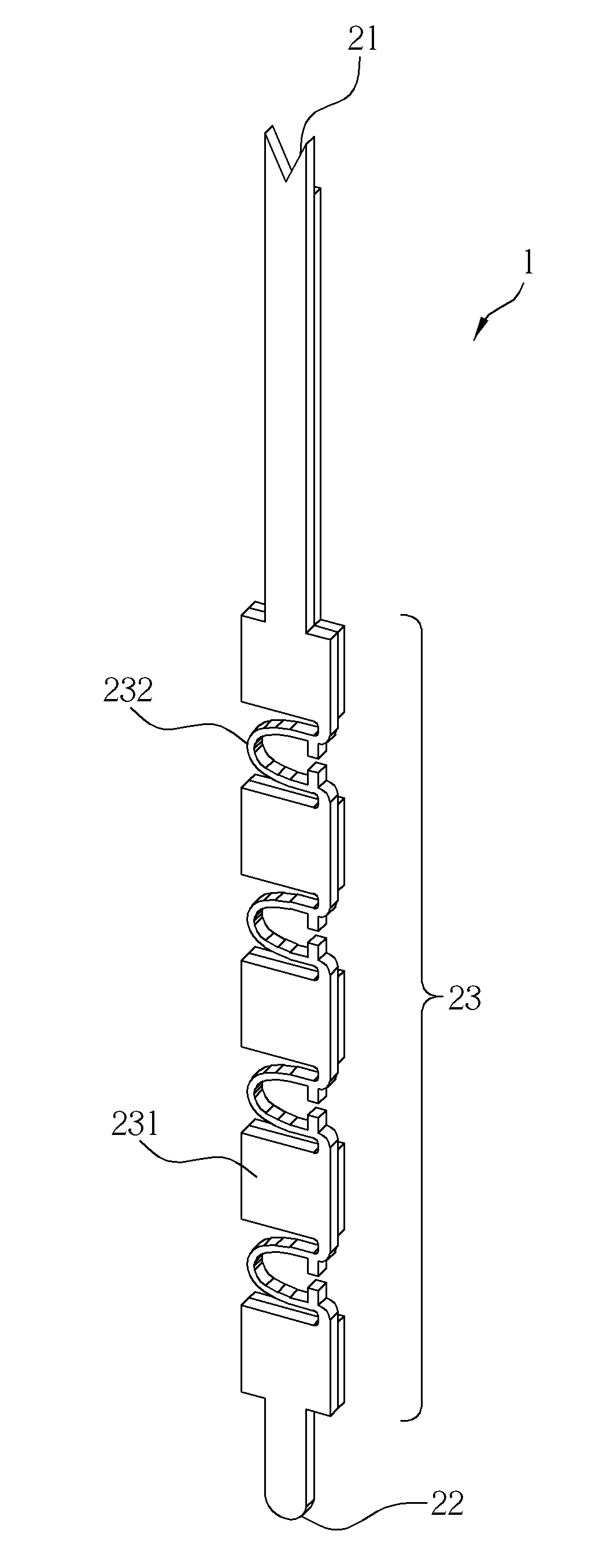
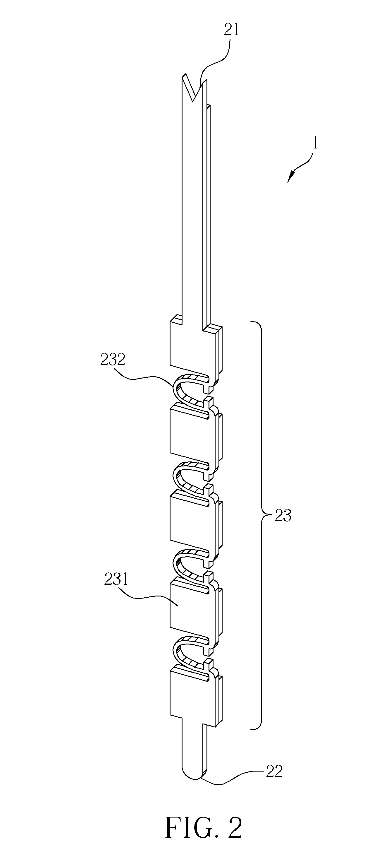
[0026]Referring to FIG. 2, FIG. 2 is a schematic assembly diagram illustrating a probe structure according to a first embodiment of the invention. The probe 1 of the invention comprises a first contact end 21, a second contact end 22 and a probe body 23. The first contact end 21 and the second contact end 22 are used for electrically contacting an external component while the probe 1 is compressed. The probe body 23 comprises a plurality of plate portions 231 and a plurality of resilient portions 232, wherein the plate portions 231 and the resilient portions 232 are connected to each other. The plate portions 231 are used for supporting deformation of the resilient portions 232 while the resilient portions 232 are compressed vertically. Furthermore, the probe 1 is flat so a plurality of probes 1 can be arranged in parallel with lateral surface (i.e. the smaller surface of the probe) . Therefore, the invention can dispose more and more probes 1 on testing components or circuit boards...


PUM


Abstract

The invention provides a high-frequency vertical spring probe card structure including a plurality of probes. Each of the probes includes at least one conducting layer and at least one insulating layer. The conducting layer includes a first contact end and a second contact end used for electrically contacting an external component while the probe is compressed and includes a probe body including at least one plate portion and at least one resilient portion connected to each other. The plate portion is used for supporting deformation of the resilient portion while the resilient portion is compressed vertically. The insulating layer includes at least one plate member tightly attached to the plate portion of the conducting layer correspondingly. The probe structure of the invention is simple and can be formed as multi-layer stack structure by electroplating through Lithographie GaVanoformung Abformung (LIGA) technology.

Description

BACKGROUND OF THE INVENTION[0001]1. Field of the Invention[0002]The invention relates to a probe structure and, more particularly, to a high-frequency vertical spring probe card structure, which is a new design of micro probe structure and can be used for testing high-frequency and high-speed chip. The probe of the invention can maintain good contact status during testing when the probe is compressed vertically.[0003]2. Description of the Prior Art[0004]In semiconductor industry, a die of a chip has to be tested by probes through related testing instrument and software before package so as to sieve good products and bad products. Afterward, the good products are delivered to package process.[0005]Since integrated circuit process advances continuously, line width and pitch between circuits are getting smaller and smaller. The probe for testing is changed from a horizontal cantilever-type probe with curved tip to a vertical probe with small diameter. The vertical probes can be arrange...

Claims


Application Information

Patent Timeline
Patent Type & Authority Applications(United States)
IPC IPC(8): G01R1/067
CPCG01R1/06722G01R1/06744
Inventor HUANG, CHENG-LUNG
Owner PLEADER YAMAICHI
Why Eureka
Try Eureka