System and method of interfacing co-processors and input/output devices via a main memory system

a main memory system and coprocessor technology, applied in the computer field, can solve the problems of preventing the use of maze sequence unlocking, i/o bottlenecks, and connecting via slower buses, and taking advantage of the significantly higher bandwidth of main memory buses

Active Publication Date: 2012-08-09
RAMBUS INC
View PDF5 Cites 216 Cited by
  • Summary
  • Abstract
  • Description
  • Claims
  • Application Information

AI Technical Summary

Problems solved by technology

However, for CPIO devices (e.g.—SSD 105) that are able to operate at higher bandwidths (e.g.—input / output data at speeds faster than that supported by the bus), connecting via the slower buses creates an I / O bottleneck.
Thus, unlike a TeraDIMM, a SATADIMM does not take advantage of the significantly higher bandwidth of the main memory bus for I / O operations.
Some of these values need to be “massaged” by the Rush before they're written because the values provided by the host may not be compatible with the TeraDIMM design (especially in a no-BIOS change scenario).
In certain circumstances, there may be a design restriction that prevents the use of maze sequence unlocks.
If the Rush returns an inverted data pattern without a correct set of ECC bits when read by the host, a read error may occur.
Additionally, the ECC bits may not be checked when data is transferred to the Rush.
The use of smaller vectors is possible, buts it may limit the applicability of the circuit to certain CPUs.
In either case, these address mappings are generally not optimized for use with a TeraDIMM.
It is recognized that there may be a challenge in meeting the required latency for DDR-3 memory systems.
Because read modify write behaviour on the part of the memory controller allows for an unknown sized portion of a given cache, line to be written, the prediction may not be accurate under in certain circumstances.
Therefore, it may be necessary (but not sufficient) for all cache lines to have been written once.
Depending on the capabilities of the SSD, it may not be possible to release a write buffer until the command is complete.
However, there are two possible causes for ECC errors: actual bit errors in the internal SRAM of the Rush and noise on the DDR-3 bus.

Method used


Image

  • System and method of interfacing co-processors and input/output devices via a main memory system
  • System and method of interfacing co-processors and input/output devices via a main memory system
  • System and method of interfacing co-processors and input/output devices via a main memory system

Examples


Embodiment Construction

Prior Art

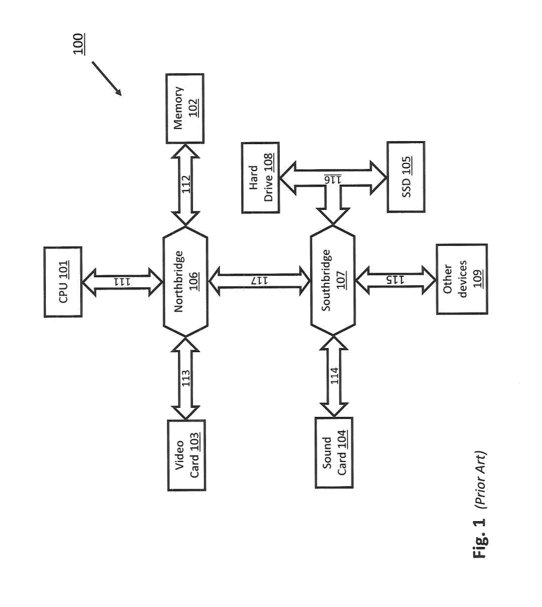
[0026]FIG. 1 illustrates a block diagram of a typical prior art computer architecture that connects co-processors or I / O (CPIO) devices via I / O buses. A computer system 100 typically includes a CPU (central processing unit) 101, a main memory unit 102 (e.g.—one or more DRAM (dynamic random access memory) modules), and CPIO devices including a video card 103, a sound card 104, a hard drive 108, and an SSD (solid state drive) 105. These components are connected together via buses on a motherboard (not shown). As illustrated, CPU 101, main memory unit 102, and video card 103 are connected via their respective buses, 111, 112 and 113, to a northbridge 106. A northbridge 106 is traditionally a chip in the chipset of the motherboard that connects high speed buses, including the FSB (front-side bus) 111, the main memory bus 112, and the PCI-E (peripheral component interconnect express) bus 113.

[0027]Slower buses, including the PCI bus 114, the USB (universal serial bus) 115, and t...


PUM


Abstract

A system for interfacing with a co-processor or input/output device is disclosed. According to one embodiment, the system includes a computer processing unit, a memory module, a memory bus that connects the computer processing unit and the memory module, and a co-processing unit or input/output device, wherein the memory bus also connects the co-processing unit or input/output device to the computer processing unit.

Description

CROSS-REFERENCES[0001]The present application claims the benefit of and priority to U.S. Provisional Patent Application No. 61 / 457,233 filed on Feb. 8, 2011, entitled “Main Memory Co-processors And Input / Output Devices,” which is herein incorporated by reference.RELATED FIELD[0002]The present disclosure relates in general to the field of computers, and in particular, to the interfacing of co-processors and input / output (I / O) devices via a main memory system.BACKGROUND[0003]A computer system utilizes multiple buses to connect various components of the computer system. The buses are physical connections that allow the various components to communicate information (e.g.—commands, addresses, and data) throughout the system. Different buses generally support different data bandwidths. For instance, a main memory bus that connects a central processing unit (CPU) to the system memory (e.g.—DRAM) can support a significantly higher data bandwidth than that supported by an I / O bus (e.g.—PCI, ...

Claims


Application Information

Patent Timeline
Patent Type & Authority Applications(United States)
IPC IPC(8): H03M13/09G06F13/36
CPCH03M13/05G06F11/1016G06F12/0246H04L9/0662G06F13/20G06F2212/7208G06F12/0607G06F13/4221G06F13/4234G06F13/404G06F13/4282G06F11/1076G06F3/0611G06F3/0619G06F3/064G06F3/0659G06F3/0673G06F9/4406H03M13/27G06F2212/1008G06F2212/1032G06F2212/7201
Inventor TAKEFMAN, MICHAEL L.AMER, MAHERBADALONE, RICCARDO
Owner RAMBUS INC
Why Eureka
Try Eureka