Solid-State Imaging Device
- Summary
- Abstract
- Description
- Claims
- Application Information
AI Technical Summary
Benefits of technology
Problems solved by technology
Method used
Image

Examples
Embodiment Construction
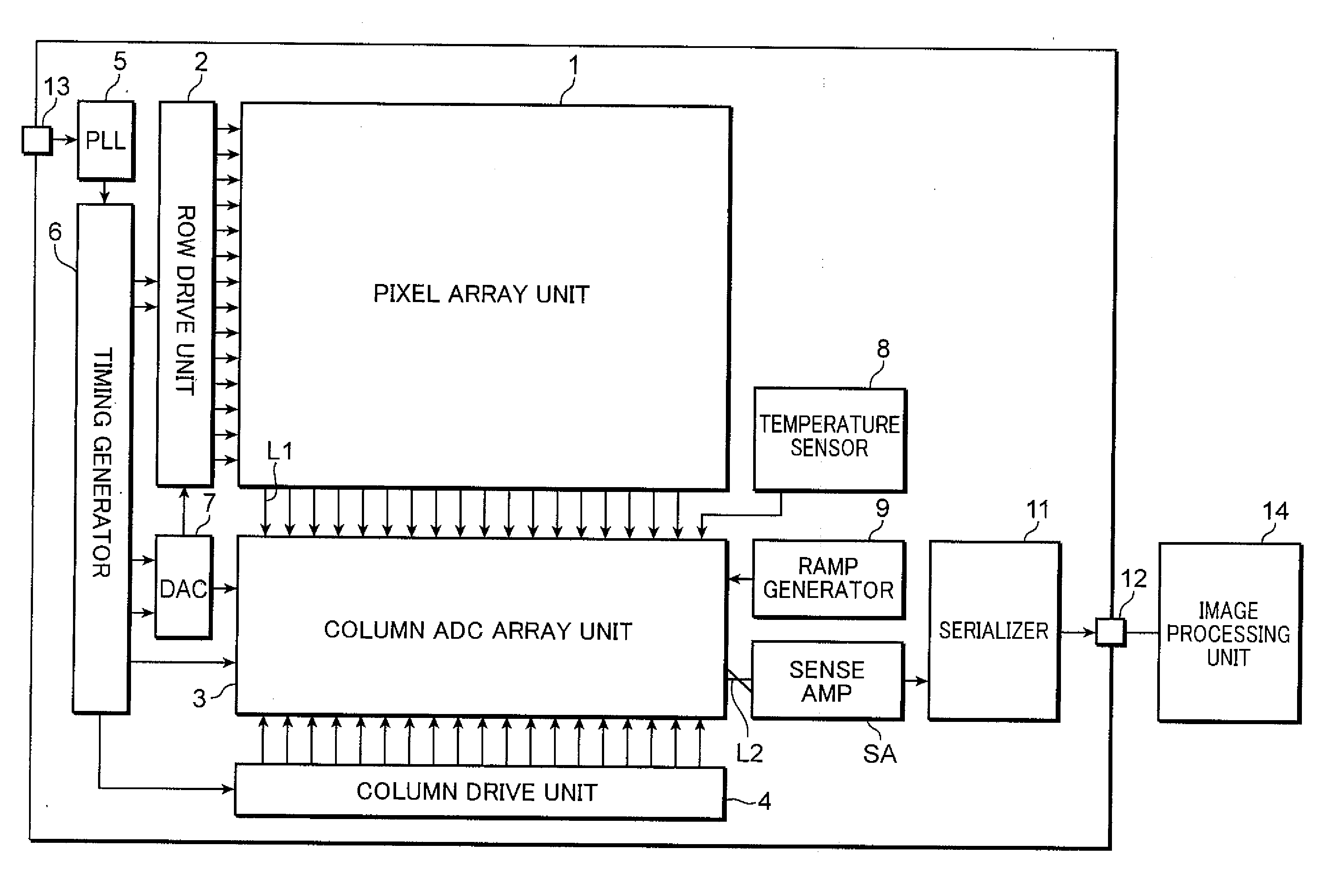
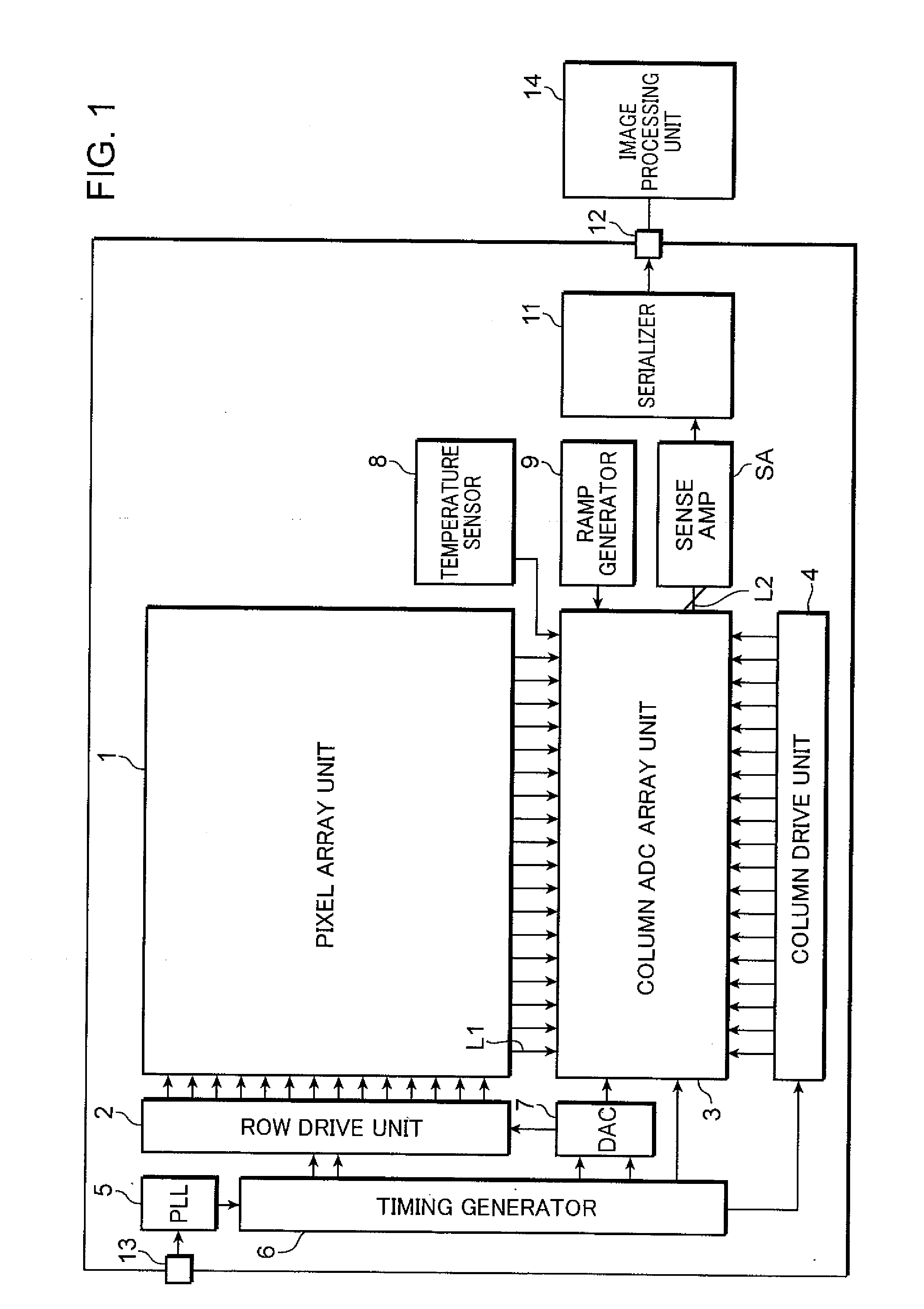
[0025]Below, the solid-state imaging device according to an embodiment of the present invention is described with reference to the drawings. FIG. 1 is a general schematic drawing of a solid-state imaging device according to an embodiment of the present invention. As shown in FIG. 1, the solid-state imaging device is a solid-state imaging device of CMOS (Complementary Metal Oxide Semiconductor) type based on a parallel column AD conversion method (column AD conversion method), comprising: a pixel array unit 1, a row drive unit 2 (one example of a vertical scanning unit), a column ADC array unit 3 (one example of a reading unit), a column drive unit 4, a PLL 5, a timing generator 6 (one example of a control unit), a DAC 7 (one example of a control unit), a temperature sensor 8 (one example of a temperature detection unit), a ramp generator 9, a sense amp SA, a serializer 11, an output terminal 12, a clock terminal 13 and an image processing unit 14.
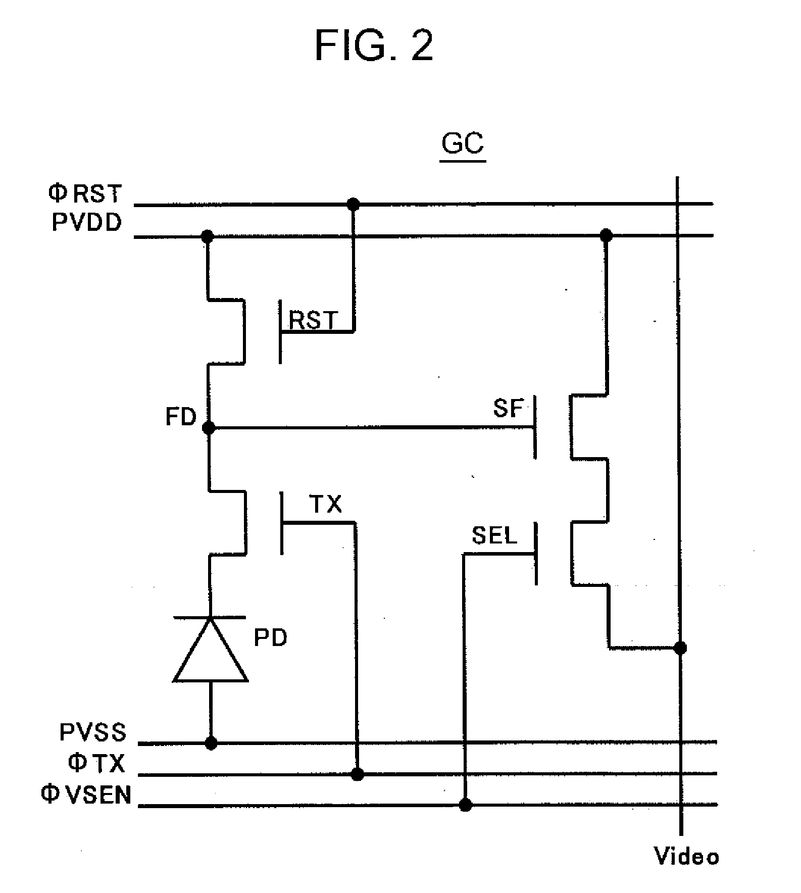
[0026]In the present embodiment, the...
PUM
 Abstract
Description
Claims
Application Information
 - Generate Ideas
- Intellectual Property
- Life Sciences
- Materials
- Tech Scout
- Unparalleled Data Quality
- Higher Quality Content
- 60% Fewer Hallucinations
Browse by: Latest US Patents, China's latest patents, Technical Efficacy Thesaurus, Application Domain, Technology Topic, Popular Technical Reports.
© 2025 PatSnap. All rights reserved.Legal|Privacy policy|Modern Slavery Act Transparency Statement|Sitemap|About US| Contact US: help@patsnap.com