
Eureka
For R&D, Eureka makes reading and utilizing patents & technical documents easy.
Eureka AIR
Designed for self-driven R&D workflows. Generate viable solutions, solve complex R&D challenges, empower your innovation with AI.

Eureka Materials
Designed for material experts only. Revolutionize your material R&D, from search, analyze, to developing new materials.

TechResearch
Generate reliable direction feasibility study reports for your R&D in just a few steps.

TechSeek
Discover and master advanced knowledge NOW. Basics, ideas, possibilities, all at once.

TechMind
As an expert in R&D Theories, TechMind can generates customized viable solutions instantly.

TechRisk
Analyze your overall solution with one click, know your potential R&D risks in advance.

TechMonitor
Get weekly tech updates, stay abreast of the latest tech innovations and key insights.
Method for producing indium tin oxide layer with controlled surface resistance
- Summary
- Abstract
- Description
- Claims
- Application Information
AI Technical Summary
Benefits of technology
Problems solved by technology
Method used
Image

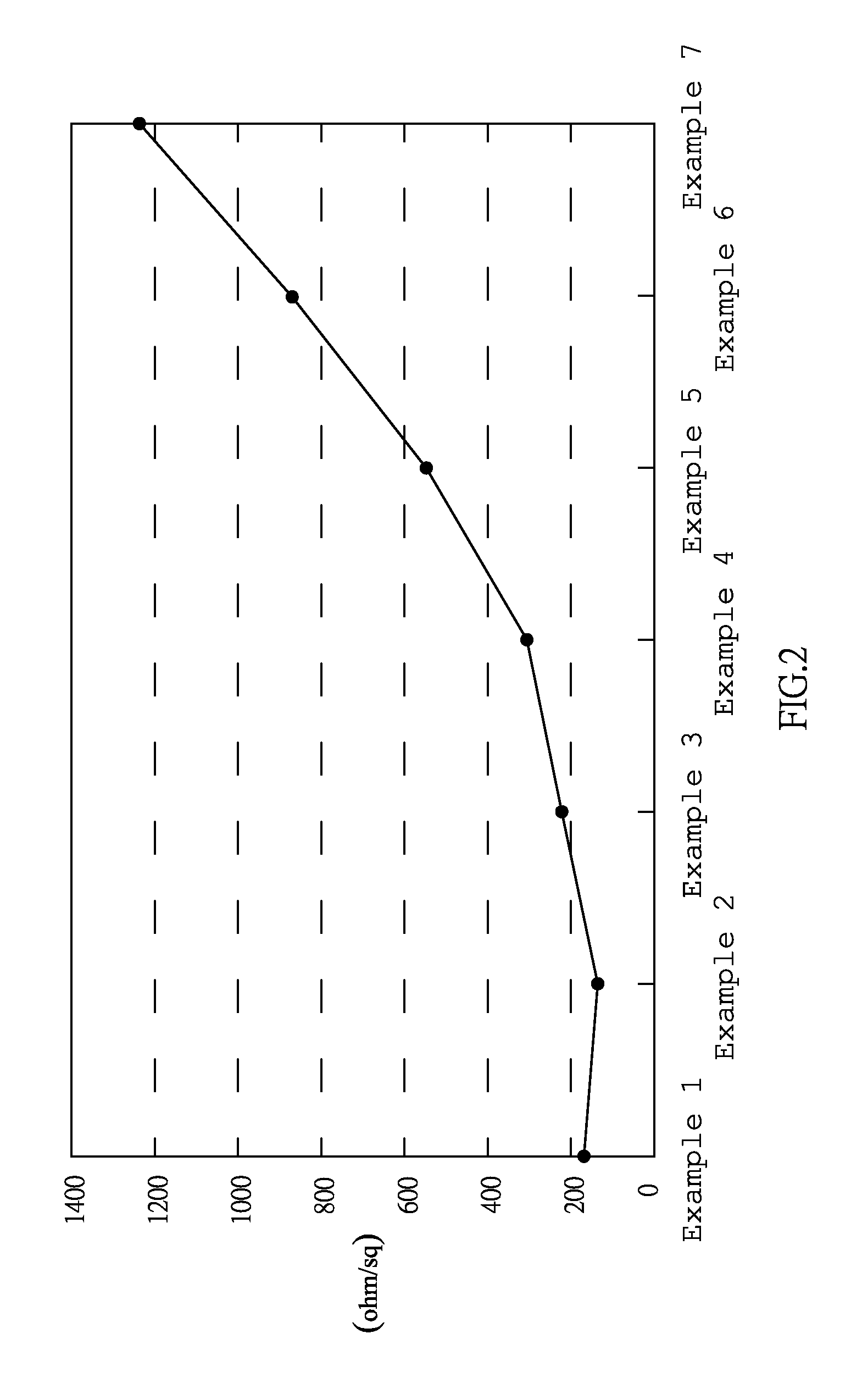
Examples
Embodiment Construction
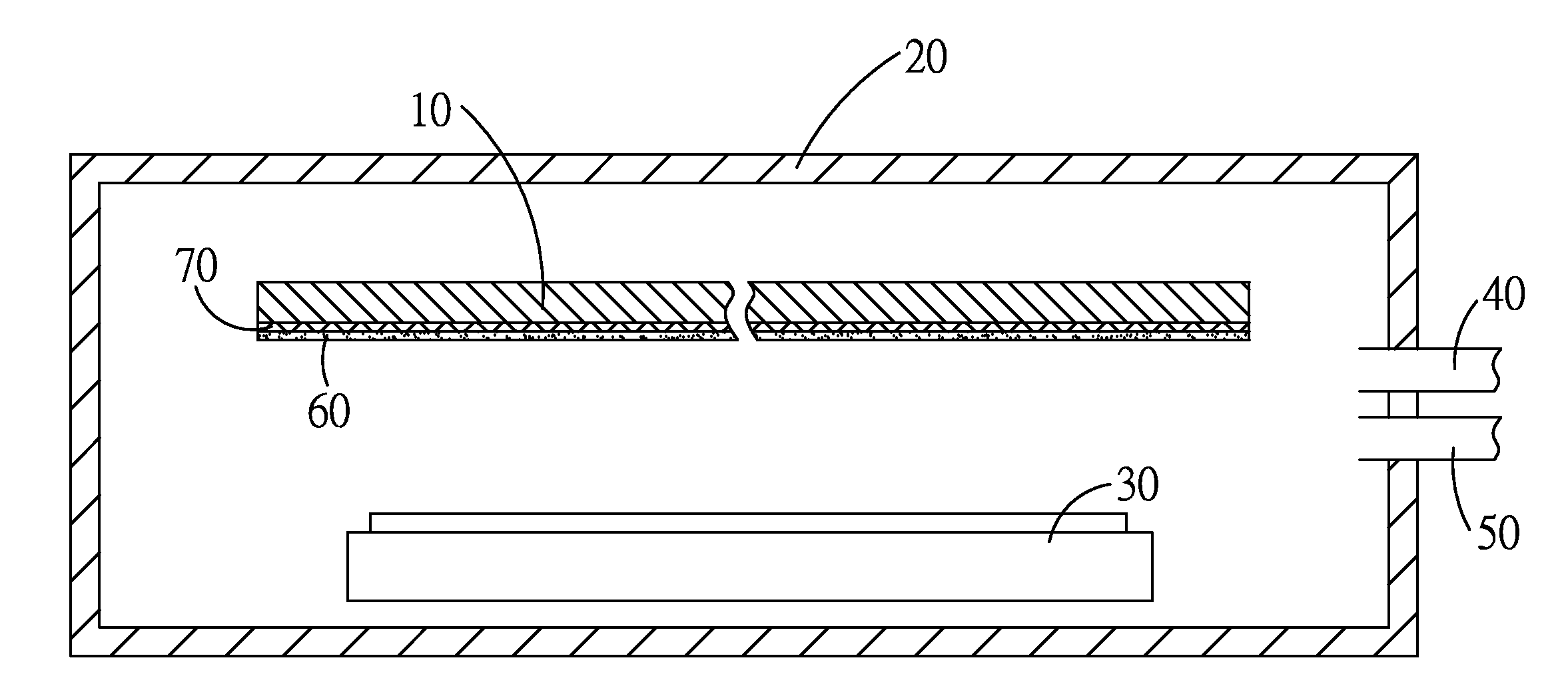
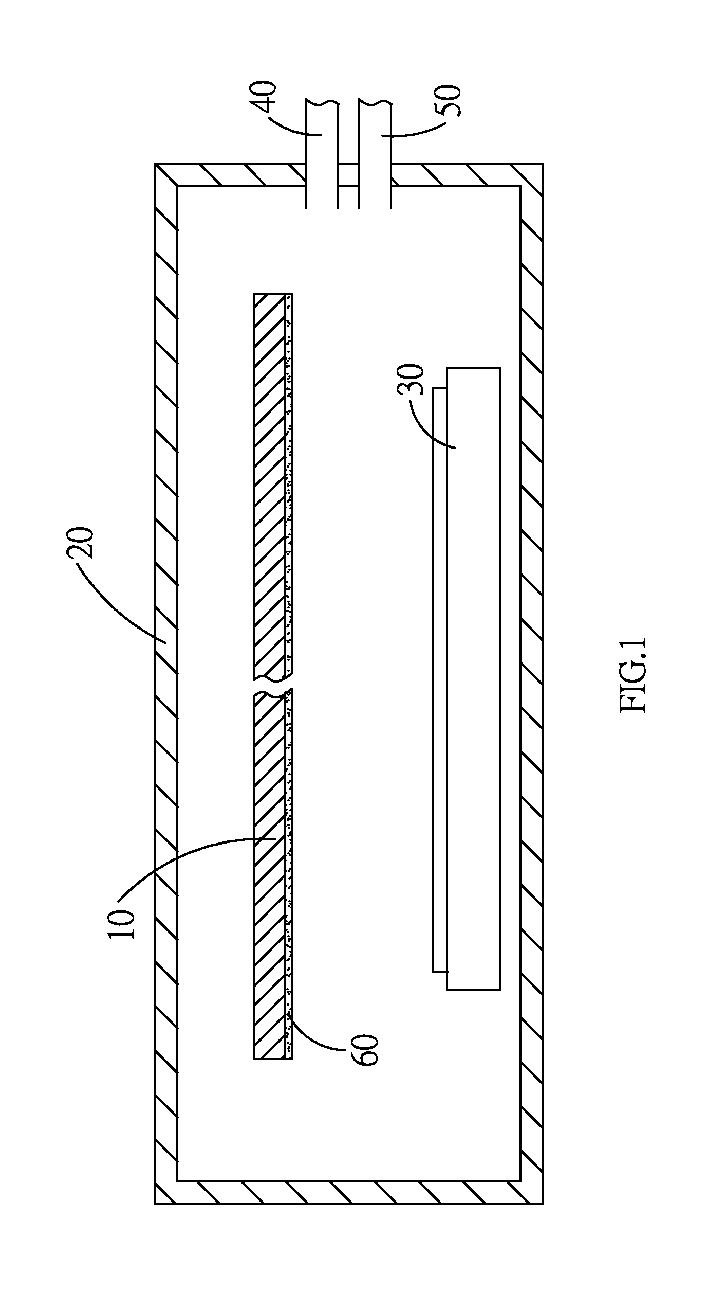
[0018]The present invention relates to a method for producing a transparent indium tin oxide conductive layer having a low value of surface resistance and a high level of uniformity. The method includes the following steps. First, as shown in FIG. 1, a substrate 10 is placed into a reaction chamber 20 of a sputtering instrument. The reaction chamber 20 is set to have a working temperature of less than 200° C. and provided inside with an indium tin oxide target 30 having a low ratio of indium oxide to tin oxide from 90%:10% by weight to 99%:1% by weight, such as a ratio of indium oxide to tin oxide from 95%:5% by weight to 97%:3% by weight. In addition, the substrate 10 may by way of example be a transparent substrate (which may be made of glass or plastic material), a thin-film transistor array substrate for a liquid crystal display device, or a substrate coated with thin films of other types.
[0019]Next, a plasma gas 40 and a reaction gas 50 are introduced into the reaction chamber ...
PUM
| Property | Measurement | Unit |
|---|---|---|
| Temperature | aaaaa | aaaaa |
| Temperature | aaaaa | aaaaa |
| Fraction | aaaaa | aaaaa |
Abstract
Description
Claims
Application Information
 - R&D Engineer
- R&D Manager
- IP Professional
- Industry Leading Data Capabilities
- Powerful AI technology
- Patent DNA Extraction
Browse by: Latest US Patents, China's latest patents, Technical Efficacy Thesaurus, Application Domain, Technology Topic, Popular Technical Reports.
© 2024 PatSnap. All rights reserved.Legal|Privacy policy|Modern Slavery Act Transparency Statement|Sitemap|About US| Contact US: help@patsnap.com