Inkjet head and inkjet plotter
a plotter and inkjet technology, applied in printing and other directions, can solve the problems of inability to downsize the inkjet head, degrade the piezoelectric substance by moisture in the air, etc., and achieve the effect of dense packing
- Summary
- Abstract
- Description
- Claims
- Application Information
AI Technical Summary
Benefits of technology
Problems solved by technology
Method used
Image
Examples
embodiments
Synthesis of a PZT Precursor Solution
[0110]After dissolving lead acetate trihydrate in methoxyethanol, the solution is dehydrated to thereby obtain a methoxyethanol solution of lead acetate trihydrate. Meanwhile, after dissolving titanium isopropoxide and zirconium isopropoxide in methoxyethanol, the solution undergoes an alcoholysis reaction and an esterification reaction. Next, the methoxyethanol solution of lead acetate trihydrate is added to it to thereby obtain a PZT precursor solution of 0.5 mol / L. In order to avoid degradation of crystallographic quality due to so-called “lead extraction” during heat processing, lead of 10 mol % is excessively added relative to the stoichiometric composition.
example 1
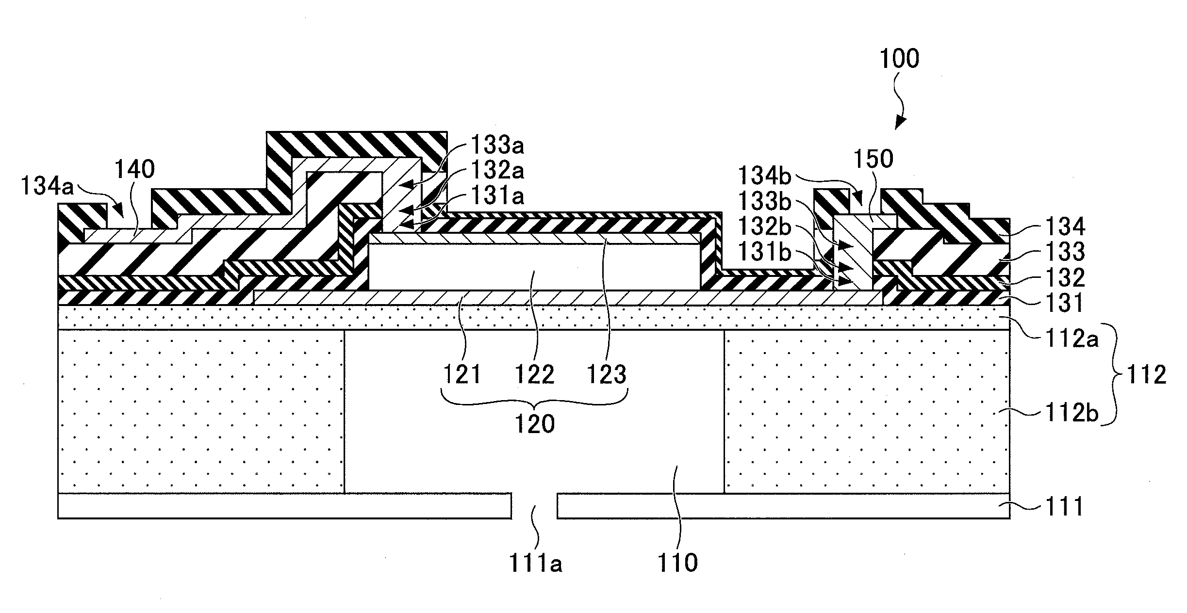
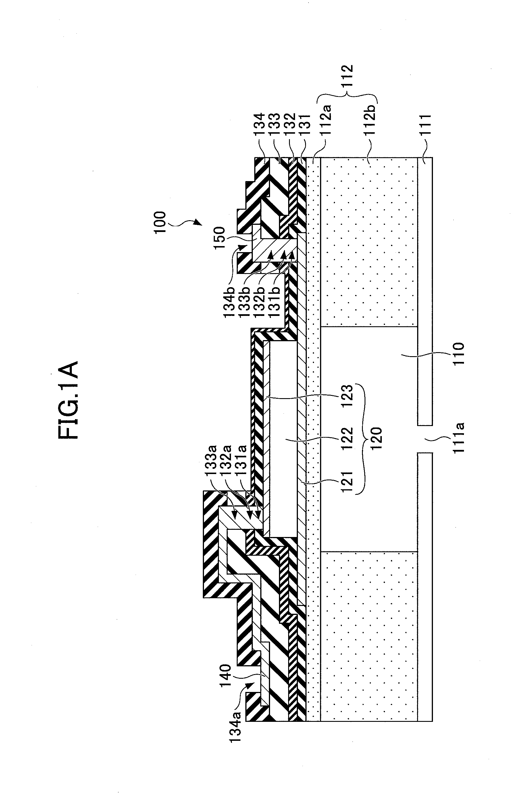
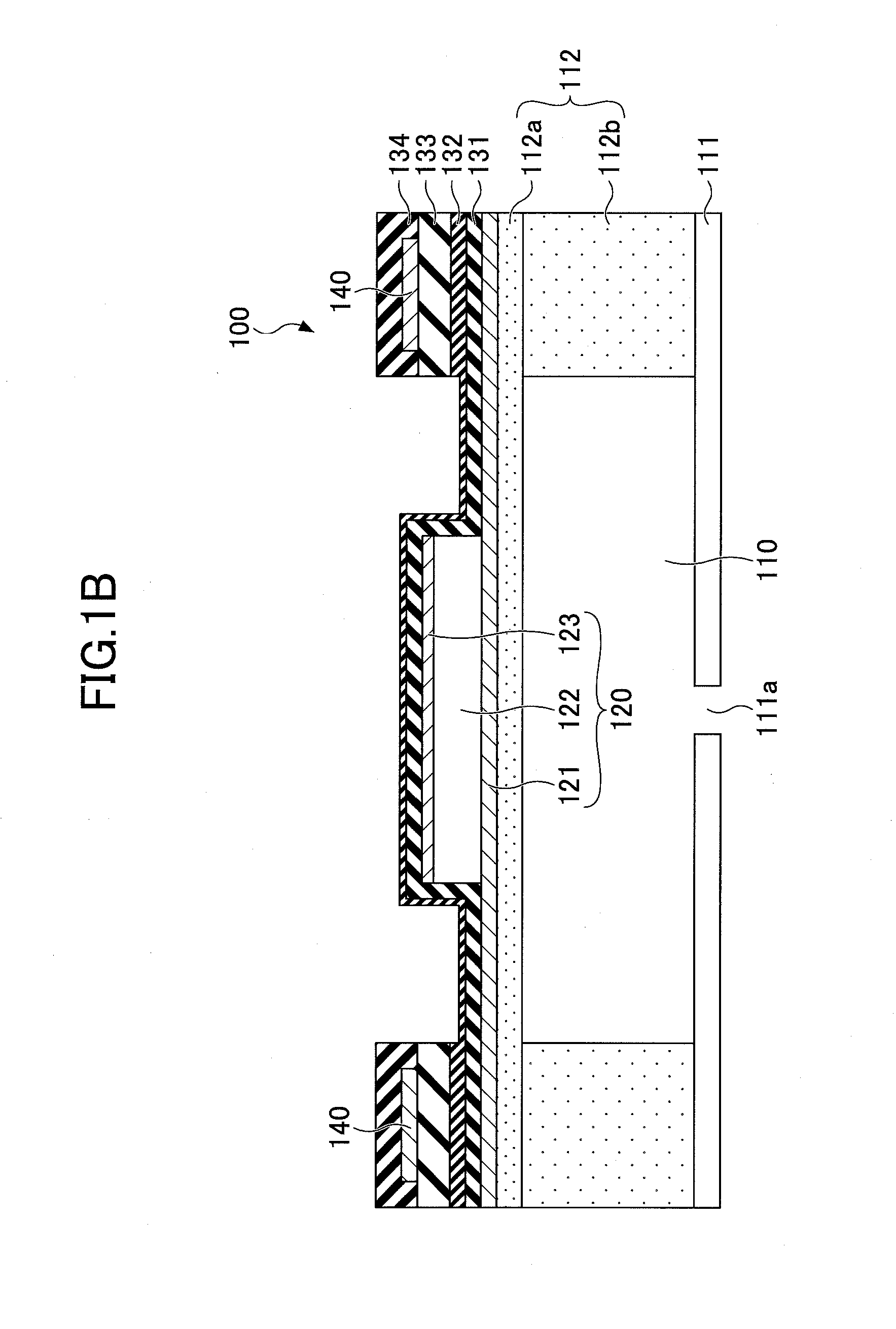
[0111]A thermally-oxidized film (the vibrating plate 112a) having a thickness of 1 μm is formed on a silicon wafer. A laminated body of a titanium film having a thickness of 50 nm, a platinum film having a thickness of 200 nm and a SrRuO3 film having a thickness of 100 nm are formed on the thermally-oxidized film by sputtering.
[0112]The PZT precursor solution is coated on the laminated body by a spin coat method, dried at 120° C. and thermally decomposed at 500° C. This process is repeated three times. Thereafter, the processed laminated body is crystallized by a rapid thermal processing (RTA) at 700° C. The above processes are repeated four times to thereby form a Pb(Zr0.53Ti047)O3 film having a film thickness of 1 μm.
[0113]Next, a laminated body of a SrRuO3 film having a thickness of 100 nm and a platinum film having a thickness of 100 nm is formed on the Pb(Zr0.53Ti0.47)O3 film.
[0114]Next, a photo resist TSMR8800 manufactured by Tokyo Ohka Kogyo Co., Ltd. is coated on the above l...
example 2
[0122]Except for the film thicknesses of 20 nm of the Al2O3 film (the insulating film 131) and the ZrO2 film (the insulating film 132), the inkjet head 100 is obtained in a similar manner to the Example 1. As a result, the film thickness of the portion without the insulating film 133 is 9 nm.
PUM
 Abstract
Description
Claims
Application Information


