Gcib process for reducing interfacial roughness following pre-amorphization

a technology of interfacial roughness and gcib, which is applied in the direction of basic electric elements, semiconductor/solid-state device manufacturing, electric devices, etc., can solve the problems of energy contamination of conventional ion implants, damage to the crystal lattice of semiconductors, and implantation process, so as to reduce the roughness of interfacial surfaces

Inactive Publication Date: 2012-10-04
TEL EPION
View PDF4 Cites 19 Cited by
  • Summary
  • Abstract
  • Description
  • Claims
  • Application Information

AI Technical Summary

Benefits of technology

[0010]The invention relates to forming an amorphous sub-layer within a portion of a substrate. In particular, methods for amorphizing layers, including silicon-containing films, on a substrate using gas cluster ion beam (GCIB) processing are described in various embodiments. More specifically, the invention relates to forming an amorphous sub-layer using a first GCIB. According to one embodiment, the method further includes using a second GCIB to reduce an interfacial roughness between the amorphous sub-layer formed using the first GCIB and a crystalline sub-layer underlying the amorphous sub-layer.

Problems solved by technology

During the conventional process of ion implantation, ionized dopant atoms are physically deposited into a crystalline semiconductor material, but it is well known that, in doing so, the crystal lattice of the semiconductor becomes damaged by the implantation process.
However, at such low energy, conventional ion implant often suffers from an energy contamination problem.
When implanting some dopants, such as boron (B), a channeling effect is unavoidable unless the silicon (Si) lattice is pre-amorphized before the dopant implant.
But Ge PAI causes implant damage, often referred to as end-of-range damage that cannot be corrected by annealing.
Such end-of-range damage results in high leakage current and other negative effect to devices.
Consequently, the impact effects of large ion clusters are substantial, but are limited to a very shallow surface region.
However, conventional GCIB processes still suffer from various deficiencies.

Method used


Image

  • Gcib process for reducing interfacial roughness following pre-amorphization
  • Gcib process for reducing interfacial roughness following pre-amorphization
  • Gcib process for reducing interfacial roughness following pre-amorphization

Examples


Embodiment Construction

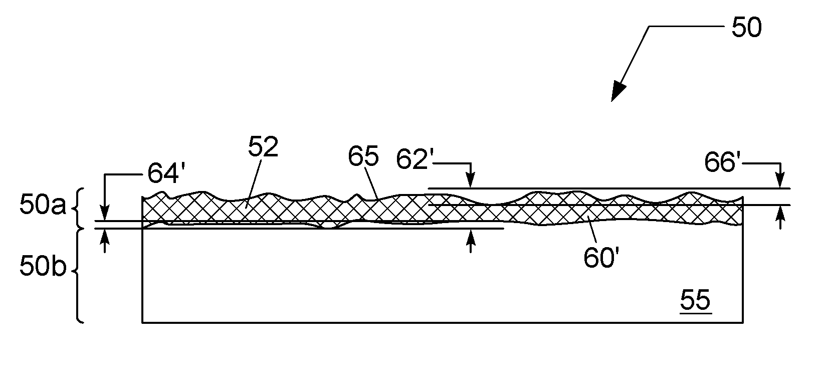
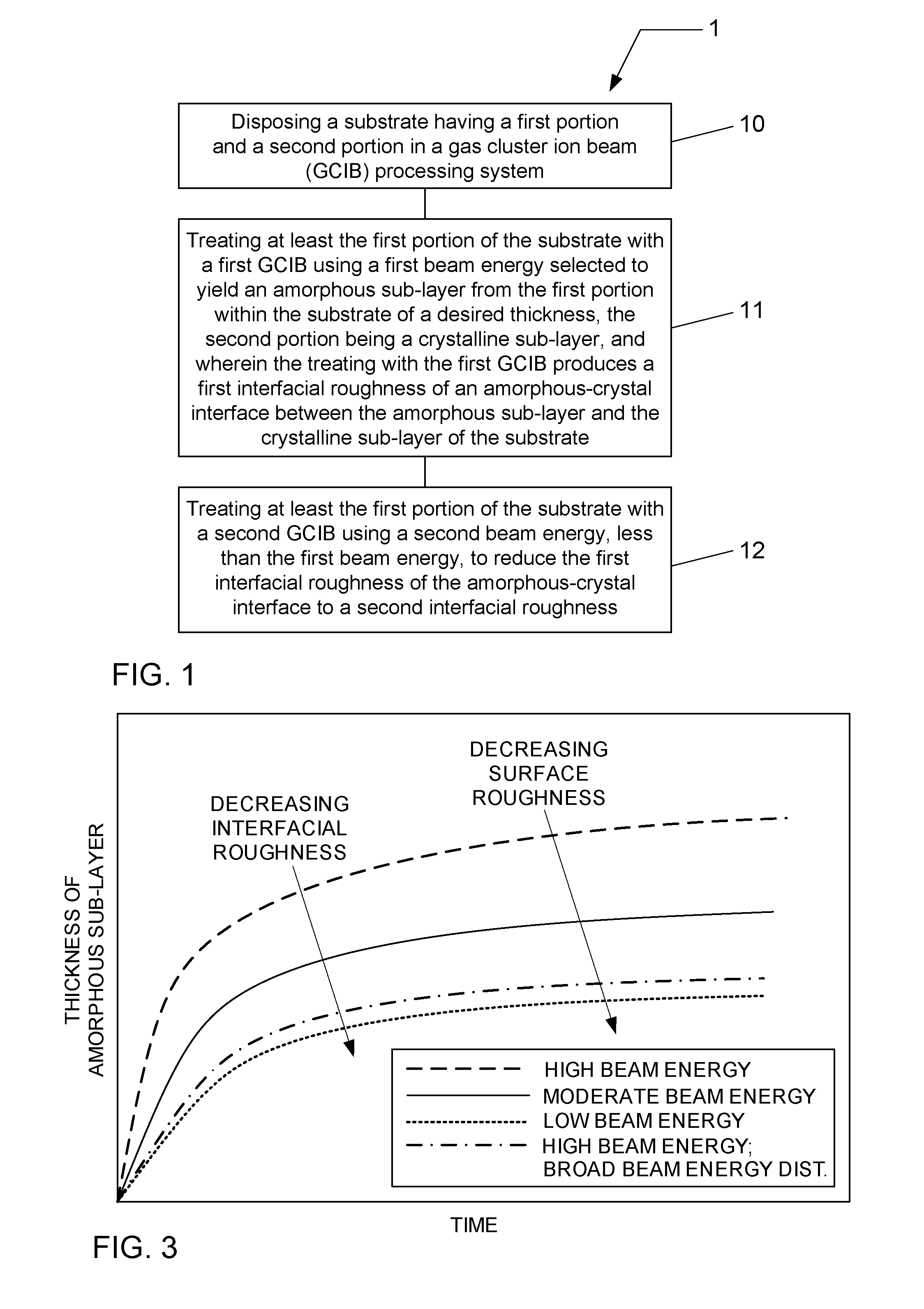
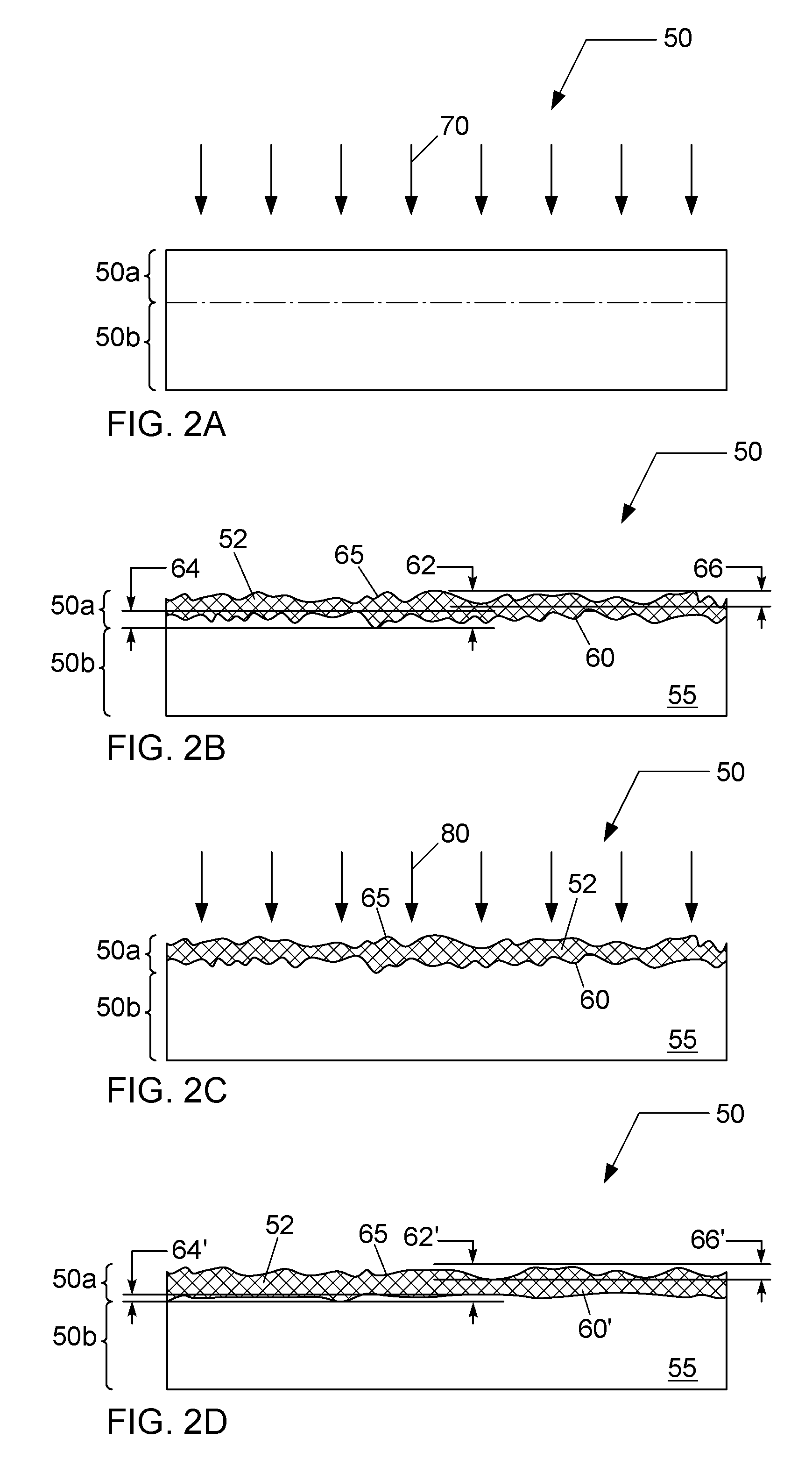
[0022]Methods for amorphizing layers, including silicon-containing films, on a substrate using gas cluster ion beam (GCIB) processing are described in various embodiments. One skilled in the relevant art will recognize that the various embodiments may be practiced without one or more of the specific details, or with other replacement and / or additional methods, materials, or components. In other instances, well-known structures, materials, or operations are not shown or described in detail to avoid obscuring aspects of various embodiments of the invention. Similarly, for purposes of explanation, specific numbers, materials, and configurations are set forth in order to provide a thorough understanding of the invention. Nevertheless, the invention may be practiced without specific details. Furthermore, it is understood that the various embodiments shown in the figures are illustrative representations and are not necessarily drawn to scale.

[0023]Reference throughout this specification t...


PUM


Abstract

A method for amorphizing a layer on a substrate is described. In one embodiment, the method includes treating the substrate with a first gas cluster ion beam (GCIB) using a first beam energy selected to yield an amorphous sub-layer within the substrate of a desired thickness, which produces a first interfacial roughness of an amorphous-crystal interface between the amorphous sub-layer and a crystalline sub-layer of the substrate. The method further includes treating the substrate with a second GCIB using a second beam energy, less than the first beam energy, to reduce the first interfacial roughness of the amorphous-crystal interface to a second interfacial roughness.

Description

BACKGROUND OF THE INVENTION[0001]1. Field of Invention[0002]The invention relates to forming an amorphous layer in a substrate.[0003]2. Description of Related Art[0004]The useful characteristics of semiconductor materials, such as silicon, germanium and gallium arsenide as well as other semiconductors, are contingent upon the purity and crystal structure of the semiconductor material. Dopant atoms incorporated into semiconductor materials for the purpose of altering electrical properties, forming electronic junctions, etc., are often introduced into a semiconductor surface by conventional ion implantation.[0005]During the conventional process of ion implantation, ionized dopant atoms are physically deposited into a crystalline semiconductor material, but it is well known that, in doing so, the crystal lattice of the semiconductor becomes damaged by the implantation process. In order for the implanted dopant atoms to become electrically active within the semiconductor and to restore ...

Claims


Application Information

Patent Timeline
Patent Type & Authority Applications(United States)
IPC IPC(8): H01L21/26H01L21/3105
CPCH01L21/26506H01L21/26566H01L21/26513H01L21/2658
Inventor GUMPHER, JOHN
Owner TEL EPION
Why Eureka
Try Eureka