Method for inspecting defects, inspected wafer or semiconductor device manufactured using the same, method for quality control of wafers or semiconductor devices and defect inspecting apparatus

a technology of defect inspection and defect inspection, which is applied in the direction of semiconductor/solid-state device testing/measurement, optical radiation measurement, instruments, etc., can solve the problems of difficult to apply such measurement to inline inspection in the manufacturing process of semiconductor devices for which high throughput is required, and the time required for measurement becomes long. , to achieve the effect of short time, easy control of displacement and stress, and sufficient accuracy

Active Publication Date: 2012-10-18
NAT INST OF ADVANCED IND SCI & TECH
View PDF12 Cites 24 Cited by
  • Summary
  • Abstract
  • Description
  • Claims
  • Application Information

AI Technical Summary

Benefits of technology

[0077]In defect inspection of an object to be inspected according to the present invention, a polarized laser beam is irradiated onto the surface of an object to be inspected, P-polarized component light and S-polarized component light of the resulting scattered light are measured simultaneously so that intensities of respective component light and a polarization direction as a ratio thereof are obtained, the intensity of each component light and polarization direction obtained in a state where no stress is applied to the object to be inspected and the intensity of each component light and polarization direction obtained in a state where stress is applied to the object to be inspected are compared respectively with a predetermined threshold value. Based on these, defects in the object to be inspected, such as internal deposits, cavity defects, surface foreign matters, scratches on the surface, or cracks in the surface layer can be detected. Further, kinds of defects can be specified and defects can be classified. Moreover, detection and classification of defects can be performed with sufficient accuracy and in a short time.
[0078]In defect inspection using application of supersonic (sonic) waves to an object to be inspected, in which it is not easy to control displacement and stress by use of resonance method and it is necessary to perform measurement for about 650 points in the range of thickness tolerance, thus requiring time for measurement of about 3 hours for inspecting defects. In contrast to this, in defect inspection according to the present invention using application of static stress, measurement is accomplished by measuring two times, that is, whether stress is applied or not. Owing to this, operation in measurement process during defect inspection becomes notably simple. Along with this, time required for measurement can be notably shortened to be several minutes and throughput in manufacturing semiconductor devices is extremely improved. With these, it is realized to perform defect inspection with in-line operation for the first time.
[0079]In such a manner, by use of a defect inspecting apparatus according to the present invention for detecting defects, specifying and classifying kinds thereof in an object to be inspected, application of static stress to the object to be inspected can be performed suitably with means of rather simple constitution. Further, inspection of defects can be accurately and efficiently and inspecting process can be accomplished in-inline manner in manufacturing semiconductor devices from wafers.
[0080]A method of detecting scattered light from an object to be inspected is employed in defect inspection according to the present invention, so that, even in the case of an object to be inspected which can not be inspected in a method by detecting transmitted light such as a wafer on which metallic wiring patterns are formed in manufacturing steps of semiconductor devices, defect inspection can be performed suitably by placing an analyzer behind the beam displacer and making rotational adjustment around the optical axis so as to remove effects of strong scattered light from metallic wiring patters or the like. Moreover, number and density of defects can be made less than a threshold value and a high yield can be attained with wafers for which the defect inspection according to the present invention has been executed.
[0081]Further, the defect inspection according to the present invention makes it possible to perform quality control through inspecting defects in a wafer, on which formation of a wiring layer and an insulator layer and flattening process are accomplished sequentially, collecting data containing number of sites exhibiting properties of polarized light intensity and polarization direction above a threshold value in the wafer surface, polarized light strength and position of polarization and displaying the data as defect distribution in the wafer surface, thus enabling quality control so as to enormously decrease non-conforming products as wafers or semiconductor devices manufactured from them.

Problems solved by technology

As an enormous number of measurement points are necessitated, time required for measurement becomes long.
As its result, throughput in manufacturing process of semiconductor devices is lowered to a large extent, thus making it difficult to apply such measurement to inline inspection in manufacturing process of semiconductor devices for which high throughput is required.
Further, equipment for changing frequency, is necessitated in resonance method of supersonic waves so that the defect inspecting apparatus becomes complicated.
Moreover, there is such a problem that impedance needs be corrected corresponding to frequencies.
Under such situation, it becomes difficult to control displacement or stress in an object to be inspected using resonance method.

Method used


Image

  • Method for inspecting defects, inspected wafer or semiconductor device manufactured using the same, method for quality control of wafers or semiconductor devices and defect inspecting apparatus
  • Method for inspecting defects, inspected wafer or semiconductor device manufactured using the same, method for quality control of wafers or semiconductor devices and defect inspecting apparatus
  • Method for inspecting defects, inspected wafer or semiconductor device manufactured using the same, method for quality control of wafers or semiconductor devices and defect inspecting apparatus

Examples


Embodiment Construction

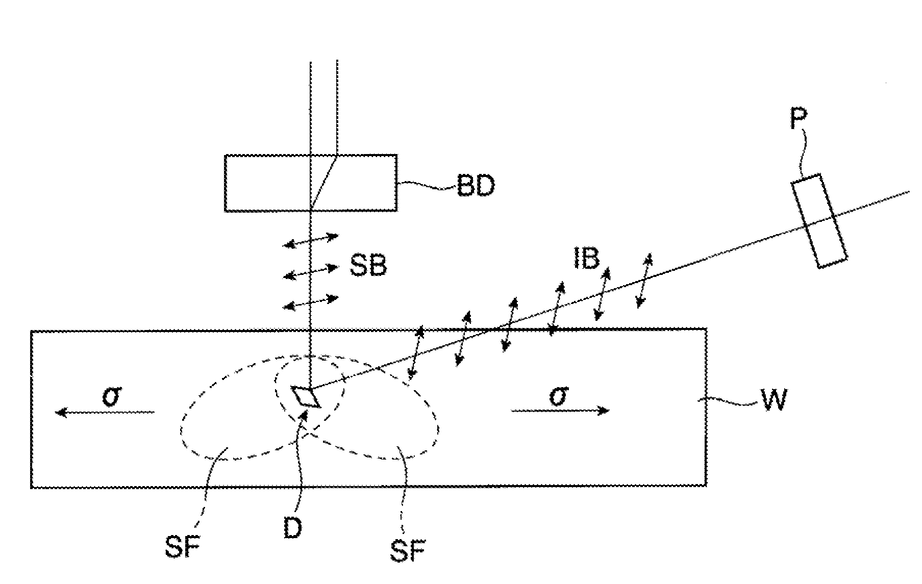
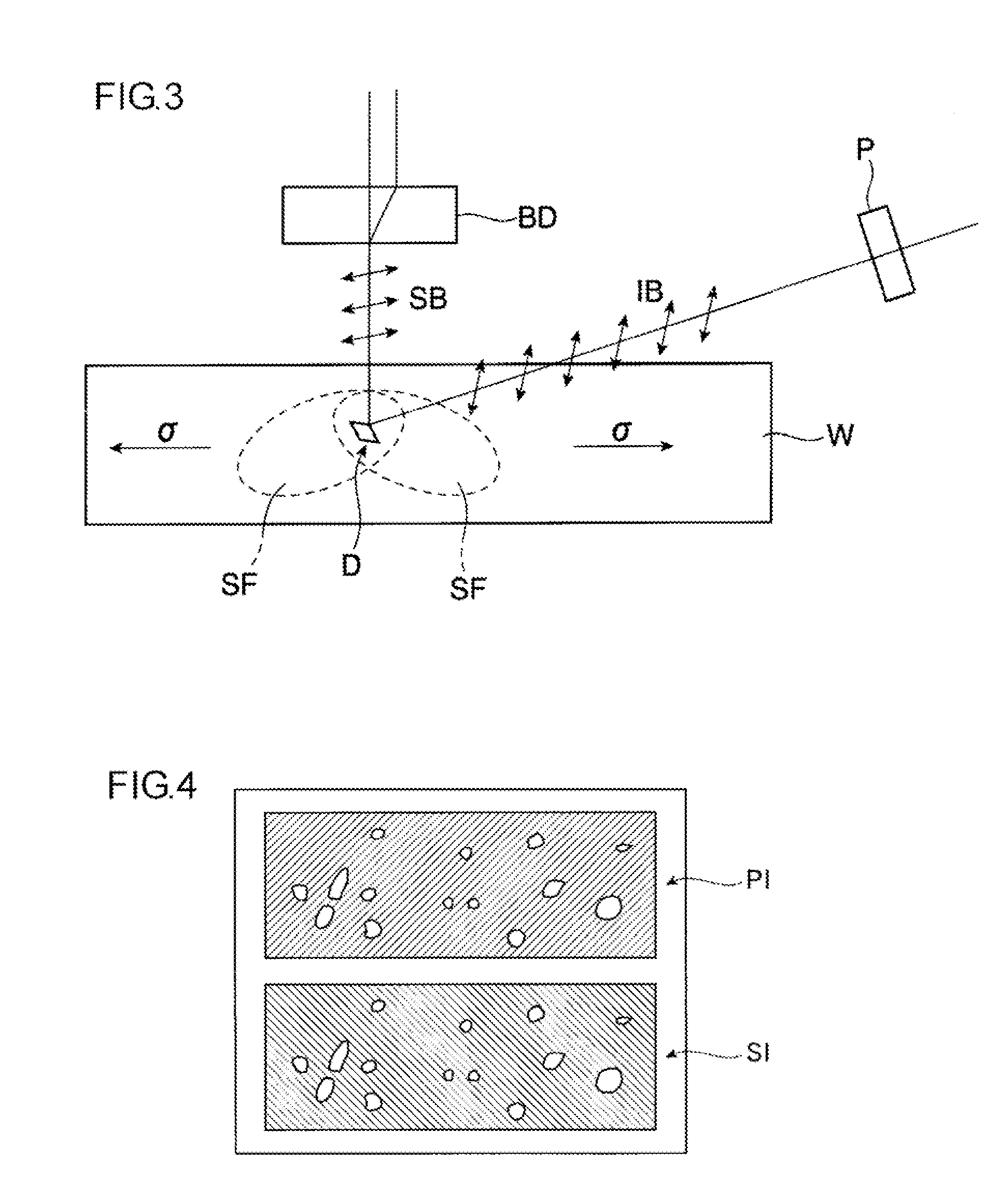
[0104] Arrangement of Defect Inspection

[0105]In the present invention, a method basically in common with one presented in Patent Document 11 as arrangement of defect inspection is used. So the arrangement of defect inspection according to the present invention containing the common method will be explained at first. In the present invention, defects are inspected through irradiating light onto the surface of an object to be inspected for which it is required to have high homogeneity, the light being of a wavelength capable of penetrating into the object to be inspected and through measuring and analyzing the scattered light of the irradiated light.

[0106]Examples of the object to be inspected include wafers for manufacturing semiconductor circuit, such as ICs or the like; substrates for manufacturing optical functional element, such as diffraction gratings; superlattice structures; MENS structures; as well as glass for liquid crystal panels and reticles, etc. High homogeneity is a ma...


PUM

PropertyMeasurementUnit
resonance frequencyaaaaaaaaaa
thicknessaaaaaaaaaa
thicknessaaaaaaaaaa

Abstract

Light from a light source device is polarized through a polarizer and is caused to impinge obliquely onto an object to be inspected. The resulting scattered light is received by a CCD imaging device having an element for separating scattered polarized light disposed in a dark field. Component light intensities are worked out for an obtained P-polarized component image and an obtained S-polarized component image and a polarization direction is determined as a ratio of them. The component light intensities and the polarization directions are determined from images obtained by imaging of the light scattering entities in a state where static stress is not applied to the object to the inspected and in a state where static load is applied thereto so as to generate tensional stress on the side irradiated by light. The component light intensities and the polarization directions are compared with predetermined threshold values.

Description

FIELD OF THE INVENTION[0001]The present invention relates to a method for inspecting defects in an object to be inspected, to a wafer for which defect inspection has been performed, to a semiconductor device manufactured using the wafer, to a method for quality control of wafers or semiconductor devices and to a defect inspecting apparatus. Specifically, the present invention relates to a method for inspecting defects through defecting and / or classifying defects in an object to be inspected such as a semiconductor wafer for which high degree of homogeneity and surface smoothness are required, to a wafer for which defect inspection has been performed, to a semiconductor device manufactured using the wafer, to a method for quality control of wafers or semiconductor devices and to a defect inspecting apparatus.BACKGROUND OF THE INVENTION[0002]In semiconductor manufacturing processes, the presence of defects inside wafers causes deterioration or impairment of electric characteristics in...

Claims


Application Information

Patent Timeline
Patent Type & Authority Applications(United States)
IPC IPC(8): G01N21/956
CPCG01N21/21G01N21/9505H01L22/12G01L1/241H01L2924/0002H01L2924/00H01L22/00G01N21/956
Inventor SAKAI, KAZUFUMINONAKA, KAZUHIROYAMAGUCHI, SHINSUKE
Owner NAT INST OF ADVANCED IND SCI & TECH
Why Eureka
Try Eureka