Method for fabricating quantum dot and semiconductor structure containing quantum dot

Inactive Publication Date: 2012-10-25
GWANGJU INST OF SCI & TECH
View PDF5 Cites 13 Cited by
  • Summary
  • Abstract
  • Description
  • Claims
  • Application Information

AI Technical Summary

Benefits of technology

[0016]As described above, according to the present invention, the quantum dot is formed by forming the dielectric thin film pattern and performing the heat treatment process, so defects may be diminished in the process of forming the quantum dot. In addition,

Problems solved by technology

However, when the etching scheme is employed, defects may occur due to the irregular atom arrangement at an edge of the quantum well structure.
In the case of the growth scheme by using the S-K mode, it is difficult to accurately adjust the growth conditions, so the size, concentration and growth position of the quantum dots may not be precisely controlled.

Method used


Image

  • Method for fabricating quantum dot and semiconductor structure containing quantum dot
  • Method for fabricating quantum dot and semiconductor structure containing quantum dot
  • Method for fabricating quantum dot and semiconductor structure containing quantum dot

Examples


fabrication example 1

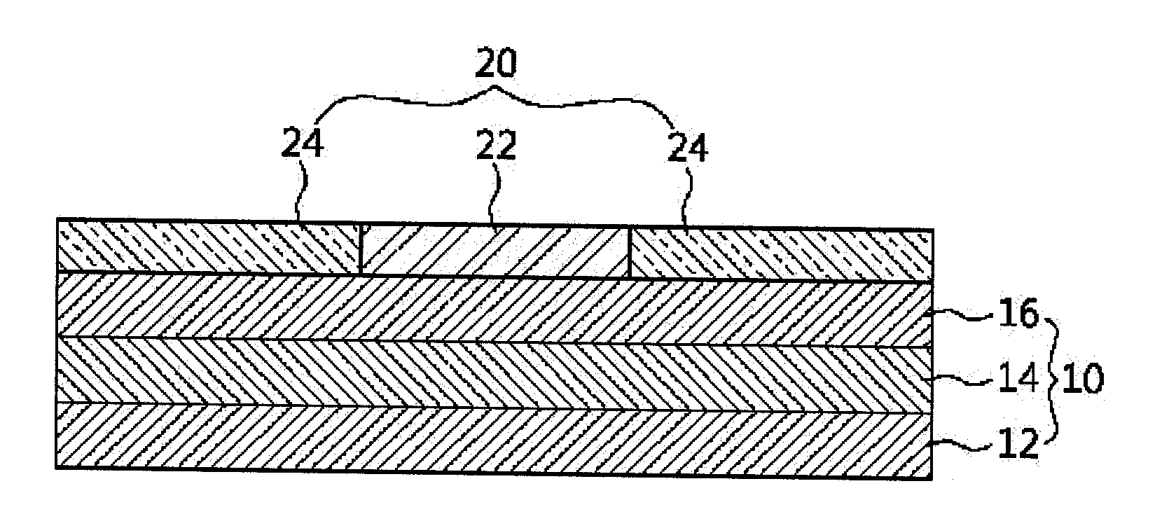
Fabrication of GaAs / AlGaAs Quantum Well

[0047]A GaAs / AlGaAs quantum well was grown through the MBE (molecular beam epitaxy).

[0048]First, a thick GaAs buffer layer was grown on a GaAs substrate, and a 20 nm Al0.45Ga0.55As clad layer, a 40-50 nm Al0.3Ga0.7As barrier layer, a 5 nm GaAs well layer, a 40-50 nm Al0.3Ga0.7As barrier layer, a 20 nm Al0.45Ga0.55As clad layer and a 5 nm GaAs cover layer were sequentially grown to form the semiconductor layer including the quantum well structure.

fabrication example 2

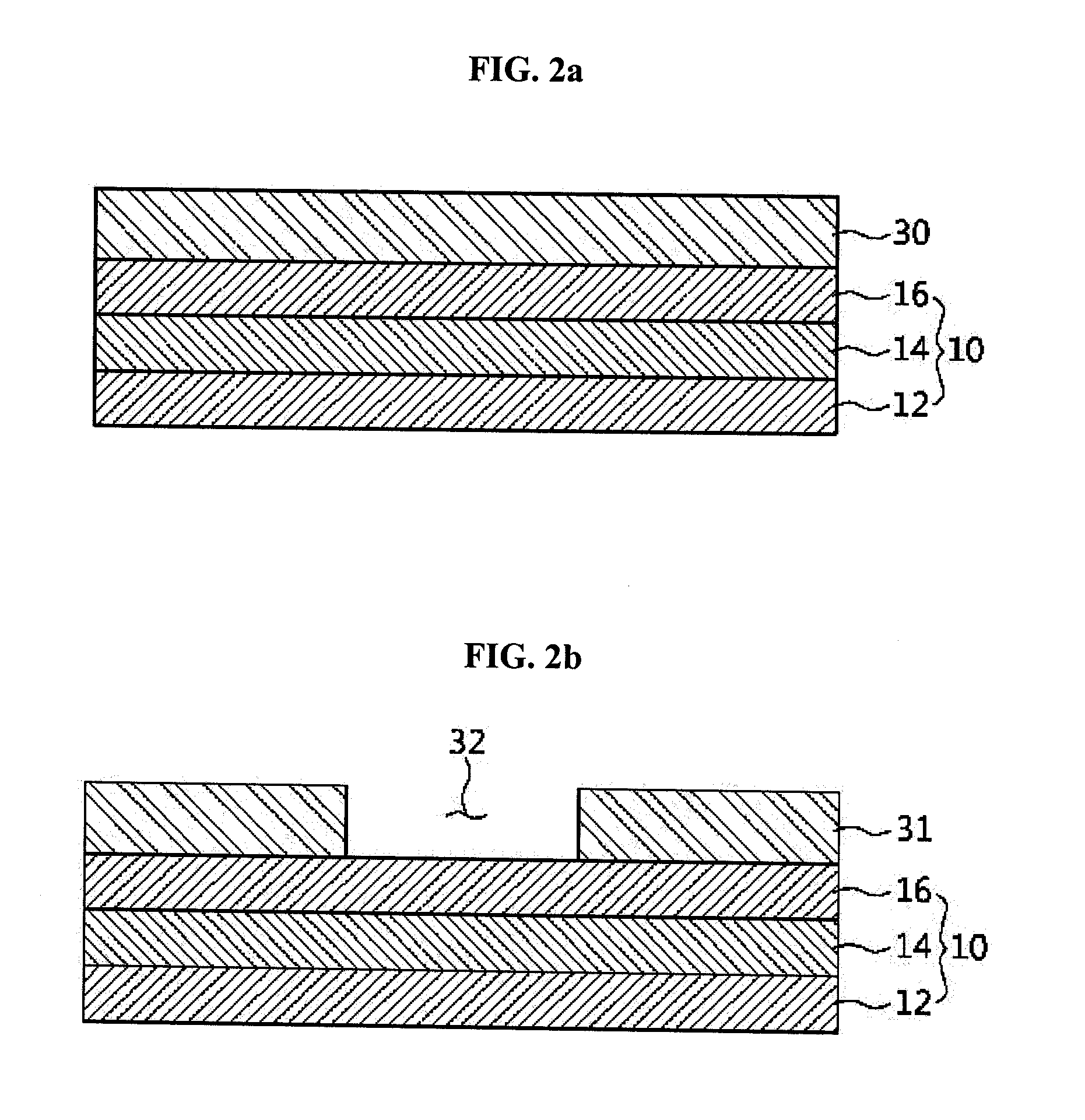
Fabrication of Dielectric Thin Film Pattern

[0049]A dielectric thin film pattern including TiO2 and SiO2 was deposited on the quantum well sample fabricated through fabrication example 1 by using the electron beam lithography and the electron beam evaporation.

[0050]1) PMMA(polymethylmethacrylate) was coated on a GaAs cover layer (thermal expansion coefficient: 6.3×10⁻⁶° C.−1) of the quantum well sample fabricated through fabrication example 1 to form a resist layer, and a part of the resist layer was etched through the electron beam lithography, thereby forming a hole pattern having a width of about 70 nm to expose a part of the cover layer.

[0051]2) 100 nm TiO2 (thermal expansion coefficient: 8.2×10⁻⁶° C.−1) was deposited on the quantum well sample having the hole pattern through the electron beam evaporation.

[0052]3) The PMMA resist layer and TiO2 formed on the resist layer were removed by using acetone.

[0053]4) 100 nm SiO2 (thermal expansion coefficient: 0.52×10⁻⁶° C.−1) was deposi...

fabrication example 3

Fabrication of Quantum Dot Through Rapid Heat Treatment Process

[0054]The quantum well sample, on which the dielectric thin film pattern including TiO2 and SiO2 was deposited, fabricated through fabrication example 2 was loaded in rapid heat treatment equipment and the quantum well sample was heat-treated for 150 seconds at the temperature of 850° C.

[0055]The micro photoluminescence of the semiconductor structure containing the quantum dot fabricated through fabrication example 3 was measured at a low temperature condition (6 K) by using an Nd:YVO4 laser having the wavelength of 532 nm.

[0056]FIG. 3 is a micro photoluminescence image of the semiconductor structure containing the quantum dot fabricated according to fabrication example 3.

[0057]FIG. 4 is a graph showing a micro photoluminescence spectrum of A and B regions shown in FIG. 3.

[0058]Referring to FIGS. 3 and 4, the photoluminescence corresponding to the quantum dot spectrum was found at the region B where the TiO2 was deposite...


PUM


Abstract

Disclosed are a method for fabricating a quantum dot. The method includes the steps of (a) preparing a compound semiconductor layer including a quantum well structure formed by sequentially stacking a first barrier layer, a well layer and a second barrier layer; (b) forming a dielectric thin film pattern including a first dielectric thin film having a thermal expansion coefficient higher than a thermal expansion coefficient of the second barrier layer and a second dielectric thin film having a thermal expansion coefficient lower than the thermal expansion coefficient of the second barrier layer on the second barrier layer; and (c) heat-treating the compound semiconductor layer formed thereon with the dielectric thin film pattern to cause an intermixing between elements of the well layer and elements of the barrier layers at a region of the compound semiconductor layer under the second dielectric thin film.

Description

CROSS-REFERENCE TO RELATED APPLICATION[0001]This application claims the benefit under 35 U.S.C. §119 of Korean Patent Application No. 10-2011-0038620, filed on Apr. 25, 2011 in the Korean Intellectual Property Office, the entirety of which is incorporated herein by reference.BACKGROUND OF THE INVENTION[0002]1. Field of the Invention[0003]The present invention relates generally to a method for fabricating a quantum dot and an application of the same. More particularly, the present invention relates to a method for fabricating a quantum dot by using a dielectric thin film pattern and a heat treatment process and a semiconductor structure containing the quantum dot fabricated through the method.[0004]2. Description of the Related Art[0005]A semiconductor quantum dot is a semiconductor structure obtained by selecting a material having a narrow bandgap from between two materials having bandgaps different from each other and growing the material in the other material having a wide bandgap...

Claims


Application Information

Patent Timeline
IPC IPC(8): H01L29/12H01L21/316B82Y40/00
CPCH01L29/127B82Y10/00B82Y40/00B82Y30/00H01L21/20
Inventor LEE, HONG SEOK
Owner GWANGJU INST OF SCI & TECH
Why Eureka
Try Eureka