Lithography system for processing a target, such as a wafer, a method for operating a lithography system for processing a target, such as a wafer and a substrate for use in such a lithography system

a lithography system and target technology, applied in the field of lithography system for processing target, can solve the problems of increasing the cost of the system, difficult to determine the position of the wafer with respect to the final projection system with a high reproducibility, system is sensitive to slight errors in the focus of light beam or tilt of the substrate, etc., to achieve easy production, high reproducibility, and easy fabrication

Active Publication Date: 2012-10-25
ASML NETHERLANDS BV
View PDF9 Cites 16 Cited by
  • Summary
  • Abstract
  • Description
  • Claims
  • Application Information

AI Technical Summary

Benefits of technology

[0018]Another advantage of this embodiment may be that this alignment sensor may be constructed in a relatively simple way with relatively small dimensions (with respect to the dimension of the final projection system).
[0143]In an embodiment the pitch between neighboring structures along the longitudinal direction follows a sinusoid function of the position of said structures along the longitudinal direction. The structures are thus arranged for smoothly varying the reflection coefficient of the position mark along the longitudinal direction.

Problems solved by technology

However, it may be difficult to determine the position of the wafer with respect to the final projection system with a high reproducibility.
A disadvantage of determining a position using light reflected in several diffraction orders is that the light detectors for the different diffraction orders have to be accurately positioned in the system, thus increasing the cost of the system.
Moreover, such systems are sensitive to slight errors in focus of the light beam or tilt of a substrate in relative to the light beam.
However, in practice the intensity distribution of the beam spot generally does not correspond to a homogeneous and sharply cut-off disc-like profile but instead follows a Gaussian profile, the resulting reflected intensity signal does not closely resemble a sinusoid function as a function of the position of the beam on the substrate.
As a result, the determination of the position of the beam spot on the substrate based on the intensity of the reflected beam is less accurate.

Method used


Image

  • Lithography system for processing a target, such as a wafer, a method for operating a lithography system for processing a target, such as a wafer and a substrate for use in such a lithography system
  • Lithography system for processing a target, such as a wafer, a method for operating a lithography system for processing a target, such as a wafer and a substrate for use in such a lithography system
  • Lithography system for processing a target, such as a wafer, a method for operating a lithography system for processing a target, such as a wafer and a substrate for use in such a lithography system

Examples


Embodiment Construction

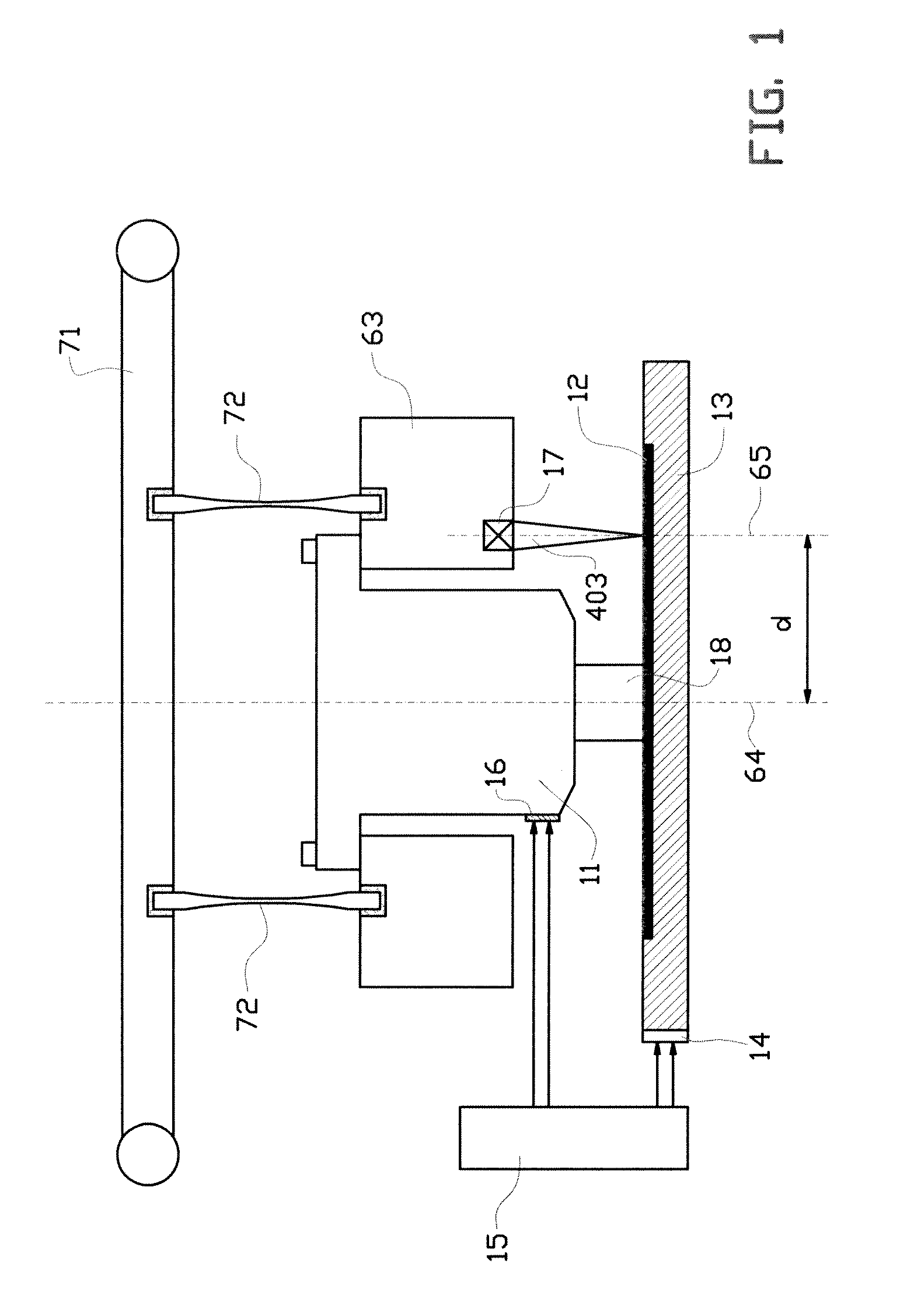
[0160]FIG. 1 shows a schematic overview of parts of embodiments of a lithography system according to the invention.

[0161]A final projection system 11 may be arranged for receiving a patterning beam from a beam source. The beam source is not shown in FIG. 1, but an example may be seen in FIG. 8. The final projection system 11 may comprise collimators, lenses or other (electro)-optical elements to shape and / or direct the patterning beam. The final projection system may be a (final) part of a projection column, the projection column comprising the beam source, deflector and other (electro)-optical elements. The projection column may be an optical projection column or a charge particle optical projection column.

[0162]The patterning beam 18 is directed towards a surface 12. This surface 12 may be surface of a target, such as a wafer or the measuring surface of a beam measurement sensor. The beam measurement sensor and / or the target / wafer may be provided on a chuck 13.

[0163]The chuck 13 m...


PUM


Abstract

The invention relates to a lithography system for processing a target, such as a wafer and a substrate for use in such a lithography system. The lithography system comprises a beam source arranged for providing a patterning beam, a final projection system arranged for projecting a pattern on the target surface, a chuck arranged for supporting the target and a mark position system arranged for detecting a position mark on a surface.

Description

[0001]According to a first aspect, the invention relates to a lithography system for processing a target, such as a wafer, and a method for operating a lithography system for processing a target, such as a wafer.[0002]Systems for processing a target are known in the art, usually comprising a final projection system for projecting a pattern on the target surface and a system for determining the position of a wafer with respect to the final projection system. In general, these systems may use position marks on the wafer. Between a first and a second session of projecting a pattern, it may be required to remove wafer from the lithography system. In that case, it may be required that the position of the pattern of the second session is matched with the position of the pattern of the first session and that the position of the wafer with respect to the final projection system (or the patterning beam) may have to be determined twice, at the beginning of each session. However, it may be dif...

Claims


Application Information

Patent Timeline
Patent Type & Authority Applications(United States)
IPC IPC(8): G03B27/54G03B27/58G03B27/32
CPCG03F9/7088G03F9/7023G03F9/7053G03F7/7085G03F7/70775G03F7/70616G03F7/70666H01J2237/30438H01J2237/31774H01J2237/2482H01L21/027G03F7/20G03F9/00
Inventor DE BOER, GUIDOVERGEER, NIELSCOUWELEERS, GODEFRIDUS CORNELIUS ANTONIUSPLANDSOEN, LAURENSVERBURG, COR
Owner ASML NETHERLANDS BV
Why Eureka
Try Eureka