Semiconductor Device and Electric Power Conversion Device Using Same

a technology of semiconductor devices and electric power conversion devices, applied in semiconductor devices, diodes, electrical apparatuses, etc., can solve problems such as current oscillation, and achieve the effect of suppressing an overcurrent and high fracture toleran

Inactive Publication Date: 2012-11-01
HITACHI LTD
View PDF3 Cites 6 Cited by
  • Summary
  • Abstract
  • Description
  • Claims
  • Application Information

AI Technical Summary

Benefits of technology

[0021]According to the present invention, an IGBT which is low-loss and low-noise (low voltage displacement, low current oscillation), has a high fracture tolerance, and suppresses an overcurrent at the time of short circuit, can be provided.

Problems solved by technology

However, in the trench gate type IGBT 11 shown in FIG. 11, there arises a problem that when the IGBT is turned on, a current oscillation occurs and an overvoltage occurs across a diode 403 (FIG. 10) connected to an IGBT 402AP (FIG. 10) in parallel.

Method used


Image

  • Semiconductor Device and Electric Power Conversion Device Using Same
  • Semiconductor Device and Electric Power Conversion Device Using Same
  • Semiconductor Device and Electric Power Conversion Device Using Same

Examples


second embodiment

of Semiconductor Device

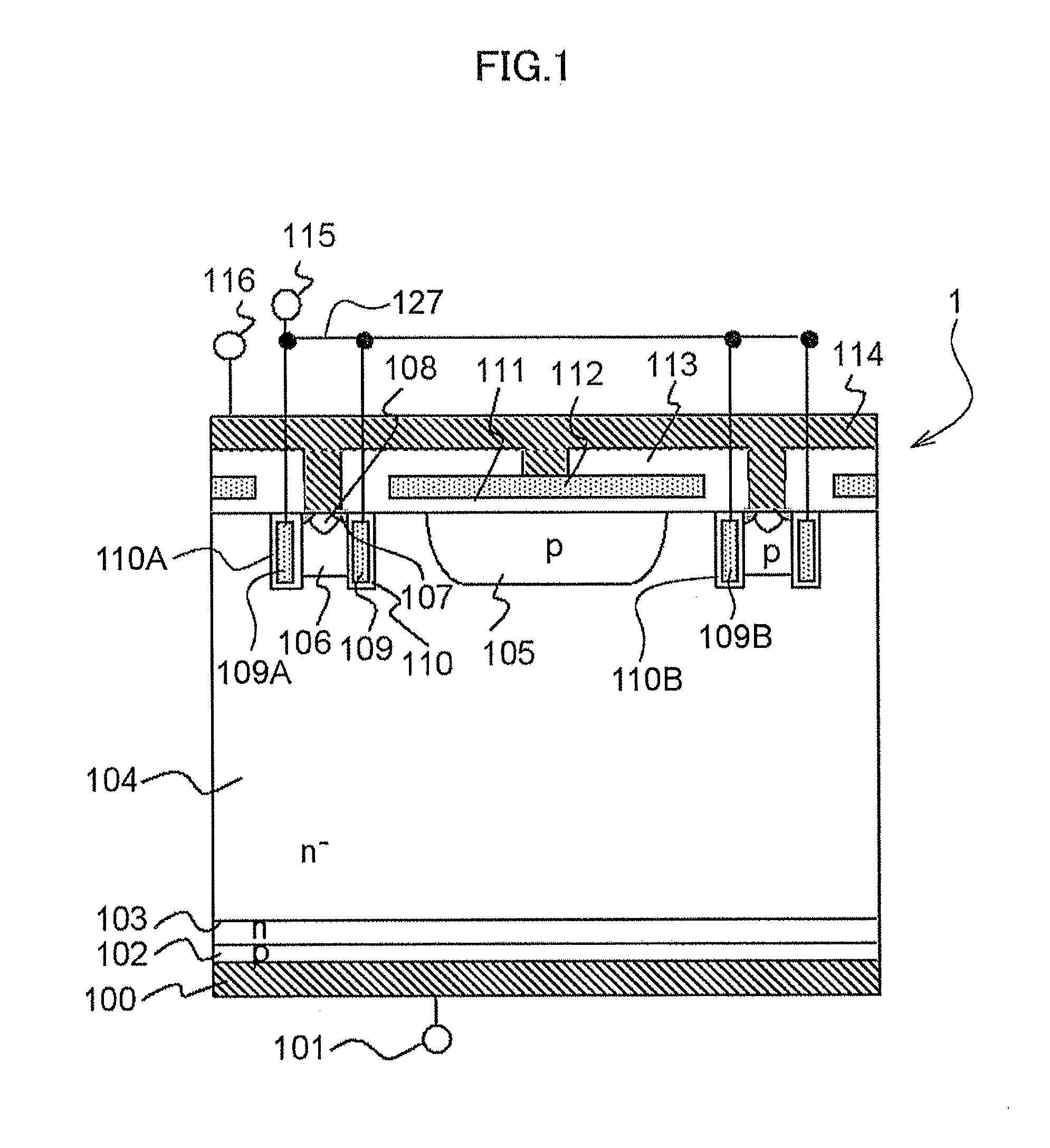
[0052]FIG. 2 is a sectional view showing a structure of a trench gate type IGBT 2 as a semiconductor device according to a second embodiment of the present invention.

[0053]In FIG. 2, the p-collector layer 102, the n-buffer layer 103, the n− drift layer 104, the p-channel layer 106, the gate electrode 109, and the n-emitter layer 107 are provided as basic components of the IGBT 2.

[0054]Also, in order to use the IGBT 2 as a practical device, the collector electrode 100, the collector terminal 101, the emitter electrode 114, the emitter terminal 116, the gate wiring electrode 127, the gate terminal 115, the gate insulating film 110, the p-contact layer 108, and the insulating film 113 are provided.

[0055]Also, in order to keep the IGBT low-noise and breakdown voltage, the floating-p layer 105, the insulating film 111, and the polycrystalline silicon 112 are provided.

[0056]Since these components are the same as those of the structure shown in FIG. 1, the explanatio...

third embodiment

of Semiconductor Device

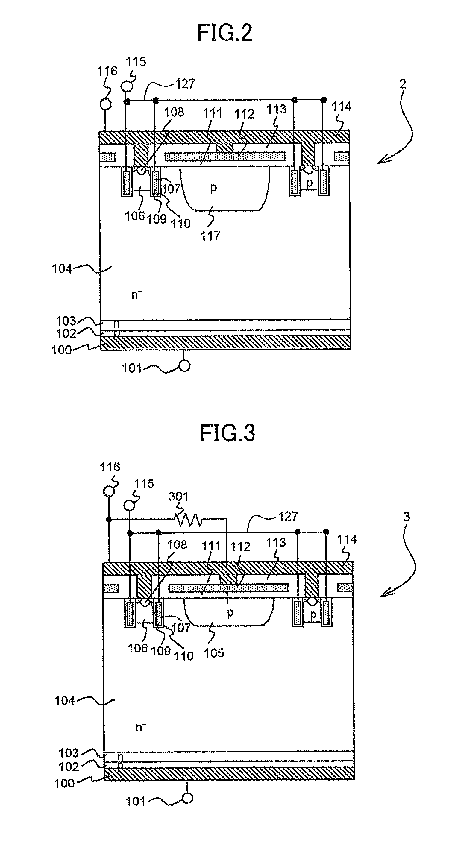
[0059]FIG. 3 is a sectional view showing a structure of a trench gate type IGBT 3 as a semiconductor device according to a third embodiment of the present invention.

[0060]In FIG. 3, the p-collector layer 102, the n-buffer layer 103, the n− drift layer 104, the p-channel layer 106, the gate electrode 109, and the n-emitter layer 107 are provided as basic components of the IGBT 3.

[0061]Also, in order to use the IGBT 3 as a practical device, the collector electrode 100, the collector terminal 101, the emitter electrode 114, the emitter terminal 116, the gate wiring electrode 127, the gate terminal 115, the gate insulating film 110, the p-contact layer 108, and the insulating film 113 are provided.

[0062]Also, in order to keep the IGBT low-noise and breakdown voltage, the floating-p layer 105, the insulating film 111, and the polycrystalline silicon 112 are provided.

[0063]Since these components are the same as those of the structure shown in FIG. 1, the explanation...

fourth embodiment

of Semiconductor Device

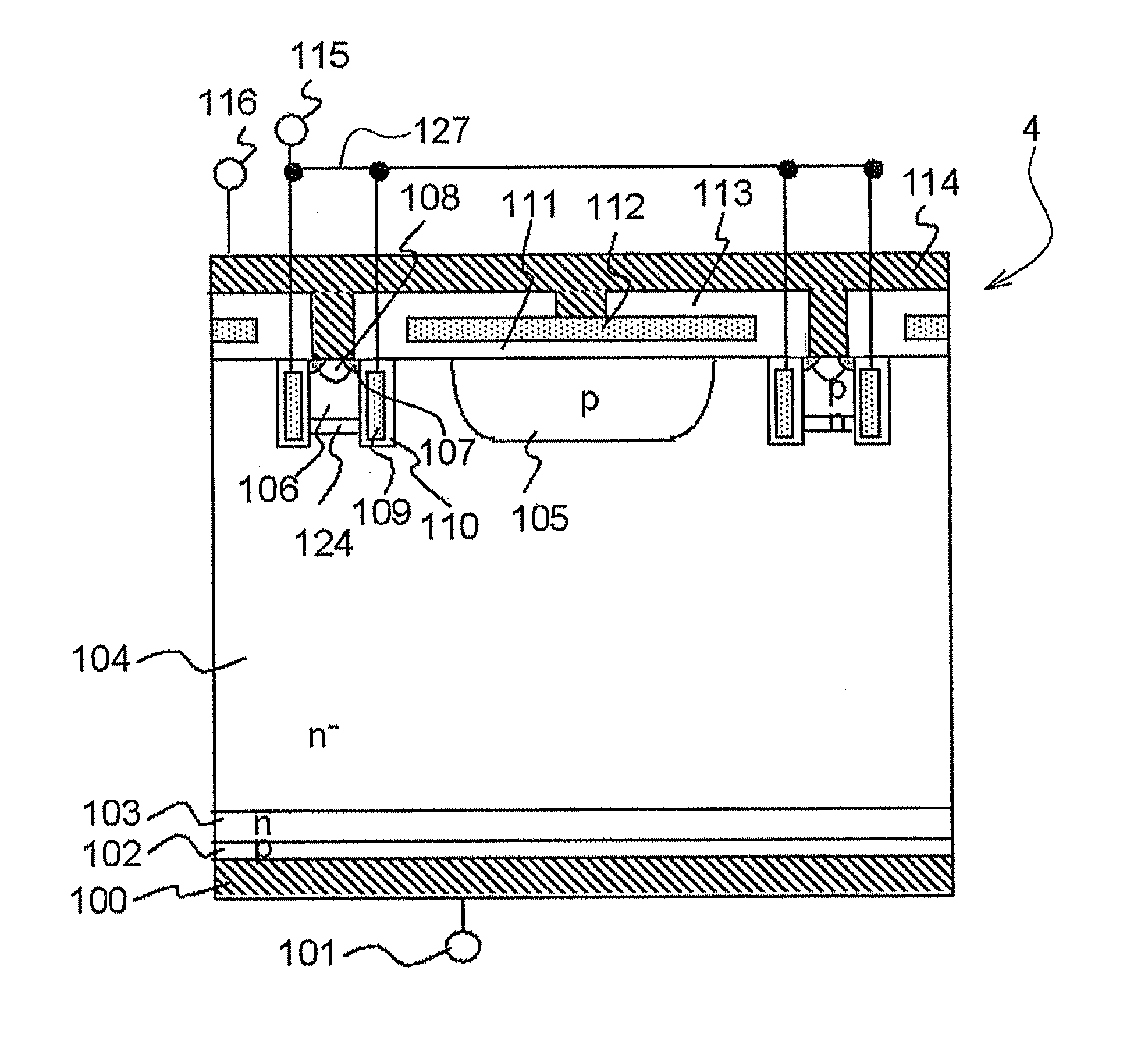
[0073]FIG. 7 is a sectional view showing a structure of a trench gate type IGBT 4 as a semiconductor device according to a fourth embodiment of the present invention.

[0074]In FIG. 7, the p-collector layer 102, the n-buffer layer 103, the n drift layer 104, the p-channel layer 106, the gate electrode 109, and the n-emitter layer 107 are provided as basic components of the IGBT 4.

[0075]Also, in order to use the IGBT 4 as a practical device, the collector electrode 100, the collector terminal 101, the emitter electrode 114, the emitter terminal 116, the gate wiring electrode 127, the gate terminal 115, the gate insulating film 110, the p-contact layer 108, and the insulating film 113 are provided.

[0076]Also, in order to keep the IGBT low-noise and breakdown voltage, the floating-p layer 105, the insulating film 111, and the polycrystalline silicon 112 are provided.

[0077]Since these components are the same as those of the structure shown in FIG. 1, the explanation...


PUM


Abstract

The trench IGBT is provided with a plurality of trench gates disposed in a manner so as to form wide and narrow of gaps; has a MOS structure that has a channel of a first conductivity type and that is between the trench gate pair that is disposed with a narrow gap therebetween; and is provided with a floating semiconductor layer of the first conductivity type and that is separated from the trench gates by interposing a portion of a third semiconductor layer of a second conductivity type between the trench gate pair that is disposed with a wide gap therebetween. Also, this floating semiconductor layer is disposed parallel to and at a position corresponding to an emitter electrode and a first semiconductor layer having the same electric potential, with a insulating film therebetween.

Description

TECHNICAL FIELD[0001]The present invention relates to a structure of an Insulated Gate Bipolar Transistor (hereinafter, referred to as an “IGBT”), and a power conversion device using the IGBT.BACKGROUND ART[0002]The IGBT is a switching element in which current flowing between a collector electrode and an emitter electrode is controlled by voltage applied to a gate electrode. Since the IGBT can control an electric power having range from several tens of watt to several hundreds of thousands of watt and has a switching frequency having wide range from several tens of Hz to several hundreds of Hz, the IGBT is widely used for low electric power equipments such as a domestic air conditioner and a microwave oven, etc. and high electric power equipments such as an inverter used for railroad and ironworks, etc.[0003]The IGBT is required to be low-loss in order to increase efficiency of the electric power equipments, and is required to decrease a conduction loss and a switching loss. Techniq...

Claims


Application Information

Patent Timeline
Patent Type & Authority Applications(United States)
IPC IPC(8): H01L27/088
CPCH01L27/0664H01L29/402H01L29/0619H01L29/0839H01L29/1095H01L29/7397
Inventor SHIRAISHI, MASAKIMORI, MUTSUHIROSUZUKI, HIROSHIWATANABE, SO
Owner HITACHI LTD
Why Eureka
Try Eureka