
LCD panel and method for forming the same

Active Publication Date: 2012-11-01
TCL CHINA STAR OPTOELECTRONICS TECH CO LTD
View PDF2 Cites 18 Cited by
  • Summary
  • Abstract
  • Description
  • Claims
  • Application Information

AI Technical Summary

Benefits of technology

[0011]An objective of the present invention is to provide a LCD liquid crystal display (LCD) panel and a method of forming the same to raising an aperture ratio of the LCD panel to improve a transmittance of the LCD panel.
[0016]In contrast to the prior art, the LCD panel and method for forming the same of the present invention can produce LCD panels with a new TFT structure using a five-mask process. In the LCD panel, a transparent conducting layer forms a first electrode and a second electrode of a TFT directly. Meanwhile, the transparent conducting layer also serves as a connecting line between a TFT and a data line and between a TFT and an LC capacitor, without forming a via hole over the TFT to link the TFT and the transparent conducting layer. In this way, an area of a pixel electrode can be further extended, and the aperture ratio of an LCD panel can be also increased, raising a transmittance of light from light sources passing through the pixel electrode.

Problems solved by technology

However, the current LCD panel having multiple transistors arranged in an active matrix is a standardized structure, which is a disadvantage of raising the frame rate.
It is too short to charge to required voltage level if considering RC delay and charging performance of TFT.
Such design reduces a aperture ratio and degrades display brightness.

Method used


Image

  • LCD panel and method for forming the same
  • LCD panel and method for forming the same
  • LCD panel and method for forming the same

Examples


first embodiment

[0032]Refer to FIGS. 6 to 14, which illustrate schematic diagrams of the LCD panel forming process according to the present invention. Firstly, refer to FIG. 6. During this stage of the forming process, firstly, a first metal layer (not shown) is deposited on a glass substrate 201. Meanwhile, a developing process is implemented through a first mask. The developing process contains the following steps: coating a photoresist (not shown) on the first metal layer, exposing the photoresist through the first mask having a specific pattern, and then washing out the exposed photoresist with a developer. Afterwards, the first metal layer undergoes an etching process. The etching process includes the steps of: removing the first metal layer, which is not covered by the photoresist, with a strong acid, producing a data line 22 on the first metal layer covered by the photoresist (roughly showing the specific pattern), and washing out the remaining photoresist.

[0033]Refer to FIG. 7. During this ...

second embodiment

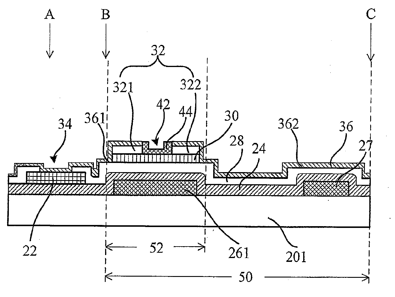
[0042]Refer to FIGS. 16 to 24, which are schematic diagrams of the LCD panel forming process according to the present invention. Firstly, refer to FIG. 16. During this stage of the forming process, firstly, a first metal layer (not shown) is deposited on a glass substrate 201. Meanwhile, a developing process is implemented through a first mask. Afterwards, the first metal layer is etched to generate a gate 261 of a switch unit and common line 27.

[0043]Refer to FIG. 17. During this stage of the forming process, firstly, a first passivation layer 24 is deposited on the glass substrate 201 and the first metal layer. Next, a second metal layer (not shown) is deposited on the first passivation layer 24. Next, a developing process is implemented through a second mask. Meanwhile, the second metal layer undergoes an etching process in order to generate a data line 22.

[0044]Refer to FIG. 18. During this stage of the forming process, firstly, an isolation layer 28 is deposited on the data lin...

third embodiment

[0056]Refer to FIG. 28 showing a layout of the pixel units according to the present invention. In contrast to FIG. 26, the data lines 22a and 22b are disposed at the same side of the of the pixel electrodes 362a and 362b. The data lines 22a and 22b are disposed in parallel and in perpendicular to the scan lines 23a and 23b. The two via holes 34a and 34b are formed over the metal layer forming the data lines and are located at the same side of the pixel electrodes 362a and 362b.


PUM


Abstract

The present invention discloses a liquid crystal display (LCD) panel and method for forming the same. In the LCD panel, the TFT includes a source and a drain formed by a transparent conducting layer, and a gate formed by a metal layer. The source is electrically connected with a data line through a via hole over the data line. The source connects to the drain via an active layer. Whatever the number of data lines are, each pixel corresponds to an associated via hole, so the number of via holes does not increase, and not reduce the aperture ratio. Therefore, the present invention is very proper to a design using more data lines and working in a high frequency. Moreover, the matrix circuitry of LCD of the present invention is well applied in a display which not only increases a density of data lines to raise the frame rate, but also maintains the aperture ratio and brightness.

Description

BACKGROUND OF THE INVENTION[0001]1. Field of the Invention[0002]The present invention relates to a liquid crystal display (LCD) panel, and more particularly, to an LCD panel and method for forming the same where a transparent conducting layer is directly connected to a data line and a thin film transistor.[0003]2. Description of Prior Art[0004]An advanced monitor with multiple functions is an important feature for use in current consumer electronic products. Liquid crystal displays (LCDs) which are colorful monitors with high resolution are widely used in various electronic products such as monitors for mobile phones, personal digital assistants (PDAs), digital cameras, laptop computers, and notebook computers.[0005]Please refer to FIG. 1 showing a layout of a pixel unit of a conventional liquid crystal display (LCD). The LCD includes a gate line 1, a data line 3, a common line 2, an active layer 6, a pixel electrode 9, and a storage capacitor 10. The pixel electrode. e.g. a transpa...

Claims


Application Information

Patent Timeline
IPC IPC(8): G02F1/136H01L33/08
CPCG02F1/136227G02F1/136286G02F2001/13629G02F2201/40G02F1/1368H01L27/124H01L27/1255G02F1/136213G02F1/13624G09G3/3648G02F1/13629G02F1/134309G02F1/136295H01L21/30604H01L21/31111H01L21/32133H01L21/76802H01L27/1218H01L27/1222H01L27/1259H01L29/66765
Inventor CHEN, CHENGHUNGHE, CHENGMING
Owner TCL CHINA STAR OPTOELECTRONICS TECH CO LTD
Features
  • Generate Ideas
  • Intellectual Property
  • Life Sciences
  • Materials
  • Tech Scout
  • Unparalleled Data Quality
  • Higher Quality Content
  • 60% Fewer Hallucinations
Learn More