Sos substrate with reduced stress
a technology of substrate and stress, applied in the direction of electrical apparatus, nanotechnology, semiconductor devices, etc., can solve the problem of excessive stress applied to silicon films, and achieve the effect of reducing the stress of silicon films
- Summary
- Abstract
- Description
- Claims
- Application Information
AI Technical Summary
Benefits of technology
Problems solved by technology
Method used
Image

Examples
example 1
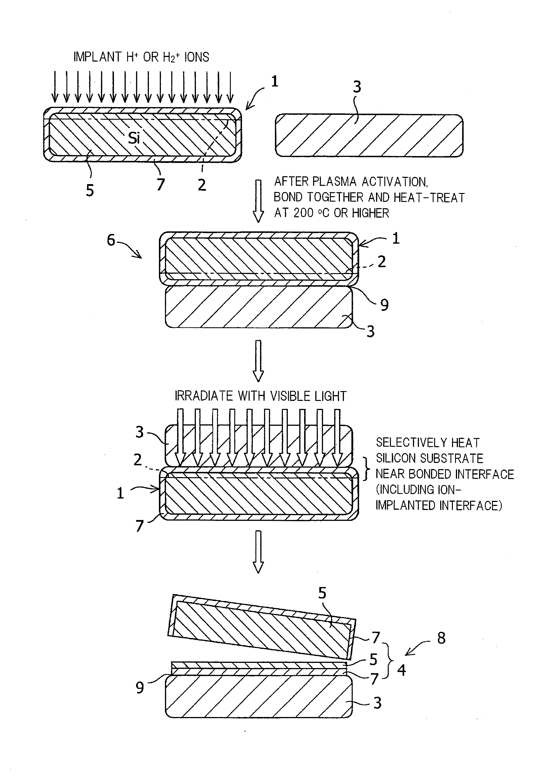
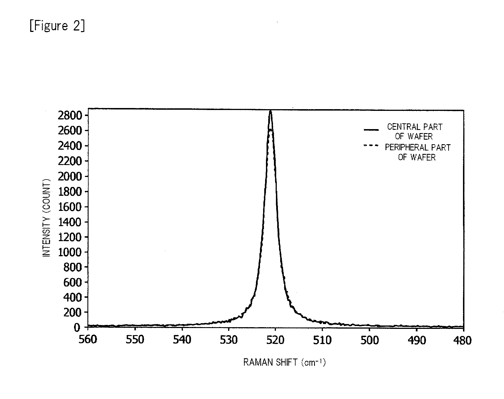
[0075]An oxide film was previously grown to a thickness of 200 nm on a silicon substrate (625 μm in thickness, 150 mm in diameter). Hydrogen ions (H+) were implanted at 55 KeV and a dose amount of 7.0×10¹⁶ atoms / cm2 into the silicon substrate. Both surfaces of a sapphire substrate and the substrate were subjected to an ion beam activation treatment and bonded together at 200° C. The substrates were heat-treated at 225° C. for 24 hours and bonded together provisionally, and then cooled to room temperature. Subsequently, the bonded substrates were placed on a 200° C. hot plate, and mechanical impact was applied to a bonded interface to cause split, thereby transferring a silicon film to the sapphire substrate. Thus, transfer of the silicon film to an entire surface of the substrate could be confirmed. A silicon layer of this substrate was CMP-polished to have a thickness of 200 nm FIG. 2 illustrates results of Raman shift measurement of the silicon film. A Raman shift in a central par...
example 2
[0076]An oxide film was previously grown to a thickness of 200 nm on a silicon substrate (625 μm in thickness, 150 mm in diameter). Hydrogen ions (H+) were implanted at 55 KeV and a dose amount of 7.0×10¹⁶ atoms / cm2 into the silicon substrate. Both surfaces of a sapphire substrate and the substrate were subjected to a plasma activation treatment and bonded together at 350° C. The substrates were heat-treated at 225° C. for 24 hours and bonded together provisionally, and then cooled to room temperature. Subsequently, the bonded substrates were heated to 300° C. on a hot plate, and mechanical impact was applied to a bonded interface to cause split, thereby transferring a silicon film to the sapphire substrate. Thus, transfer of the silicon film to the entire surface of the substrate could be confirmed A silicon layer of this substrate was CMP-polished to have a thickness of 200 nm. A Raman shift in a central part was 521.28 cm−1, and a Raman shift in a peripheral part was 521.10 cm−1....
example 3
[0077]An oxide film was previously grown to a thickness of 200 nm on a silicon substrate (625 μm in thickness, 150 mm in diameter). Hydrogen ions (H+) were implanted at 55 KeV and a dose amount of 7.0×10¹⁶ atoms / cm2 into the silicon substrate. Both surfaces of a sapphire substrate and the substrate were subjected to a plasma activation treatment and bonded together at 200° C. The substrates were heat-treated at 225° C. for 24 hours and bonded together provisionally, and then cooled to room temperature. Subsequently, the bonded substrates were heated to 250° C. on a hot plate and irradiated with a YAG laser of 523 nm in wavelength. Mechanical impact was applied to a bonded interface to cause split, thereby transferring a silicon film to the sapphire substrate. Thus, transfer of the silicon film to the entire surface of the substrate could be confirmed. A silicon layer of this substrate was CMP-polished to have a thickness of 200 nm. A Raman shift in a central part was 521.25 cm−1, an...
PUM
 Abstract
Description
Claims
Application Information