Semiconductor variable capacitor

a variable capacitor and semiconductor technology, applied in the field of semiconductor capacitor structure, can solve the problems of inability to obtain an extremely high capacitance value, inability to add unacceptable levels of inter-modulation, and limited dynamic range, so as to improve the performance of the device, avoid distortion, and change the capacitance

Active Publication Date: 2012-11-08
QUALCOMM INC
View PDF7 Cites 26 Cited by
  • Summary
  • Abstract
  • Description
  • Claims
  • Application Information

AI Technical Summary

Benefits of technology

[0018]The present invention describes a semiconductor variable capacitor MOS structure suitable for integrated circuits, which has at least three terminals, one of which is used to modulate the equivalent capacitor area of the MOS structure by increasing or decreasing its DC voltage with respect to another terminal of the device, in order to change the capacitance over a wide range of values. Furthermore, the present invention

Problems solved by technology

Their use is limited to low signal amplitudes to avoid obvious distortions as the capacitance would be affected by the change of signal voltage, precluding their use in the input stages of high-quality RF communications receivers, where they would add unacceptable levels of inter-modulation.
At VHF/UHF frequencies, e.g. in FM Radio or TV tuners, dynamic range is limited by noise rather than large signal handling requirements, and varicaps are commonly used in the signal path.
Furthermore an extremely high value of capacitance cannot be obtained even with a reverse bias because the reverse-biased saturation current is not exactly equal to zero.
This leads to the disadvantage that the AC voltage is superimposed upon the DC control value, and therefore the capacitance value is distorted by the AC voltage.
As underlined by the author himself in the patent, they are not suitable for integrated circuits.
I

Method used


Image

  • Semiconductor variable capacitor
  • Semiconductor variable capacitor
  • Semiconductor variable capacitor

Examples


Embodiment Construction

A FIG. 1

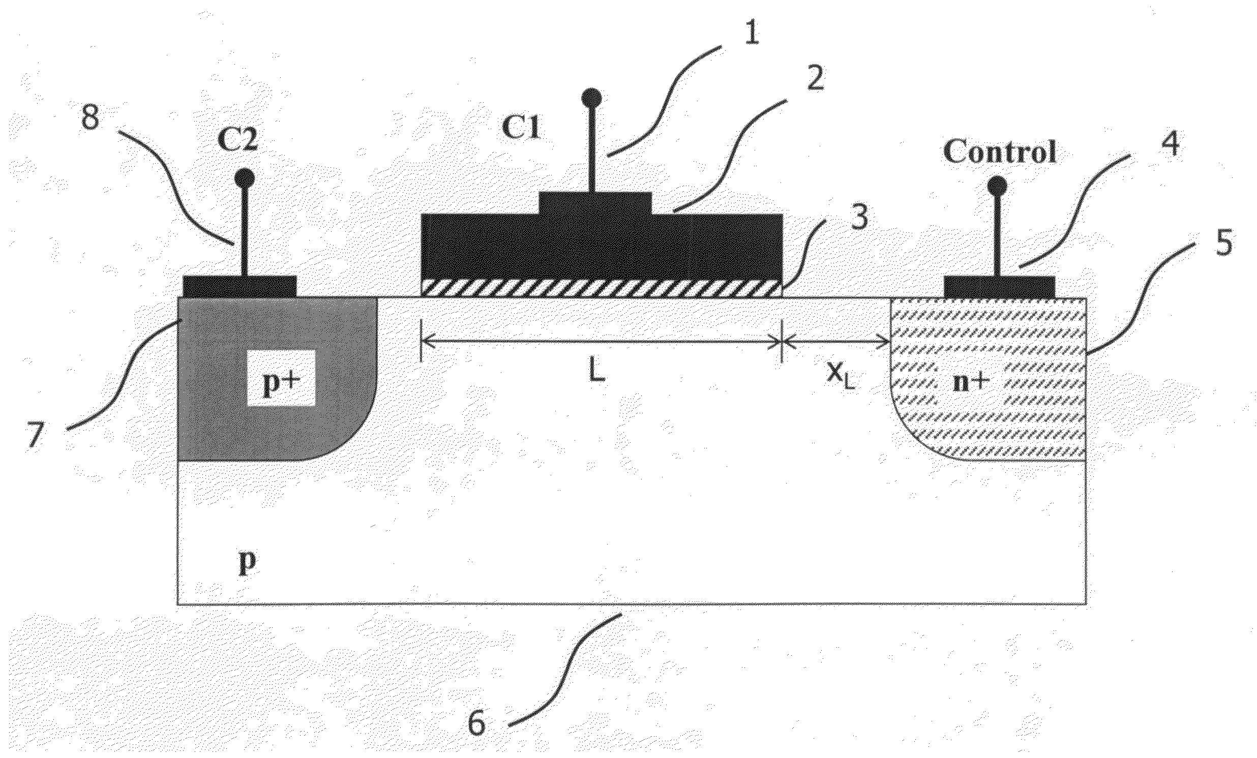
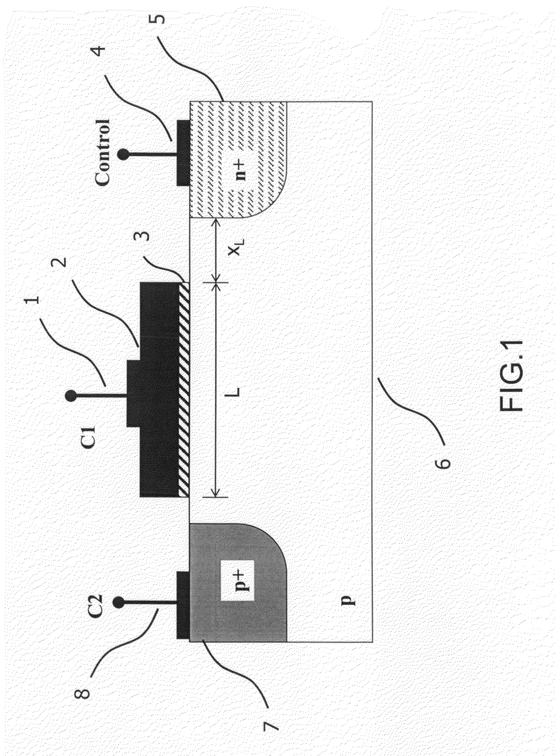
[0100]FIG. 1 is showing the first embodiment of the invention. The n+-type region 5 defines the control terminal of the device whereas the region 2 and the p+ region 7 are the two terminals of the capacitor. The regions 3 corresponds to the capacitor dielectric layer, and region 6 is the p-type substrate of the device. xL is the distance between the capacitance plate 2 and the n+ control region 5, whereas L is the length of the upper capacitance plate 2. The lower capacitance plate is constituted by the substrate 6, and is connected to the C2 terminal 8 through the p+ region 7. The C1 electrode (or terminal) 2 may be built in poly-silicon or metal.

[0101]As it can be seen, the structure is very simple and the DC control voltage, which is applied between the control terminal 4 and the C2 terminal 8, never alters the DC voltage between the two main electrodes of the MOS capacitor.

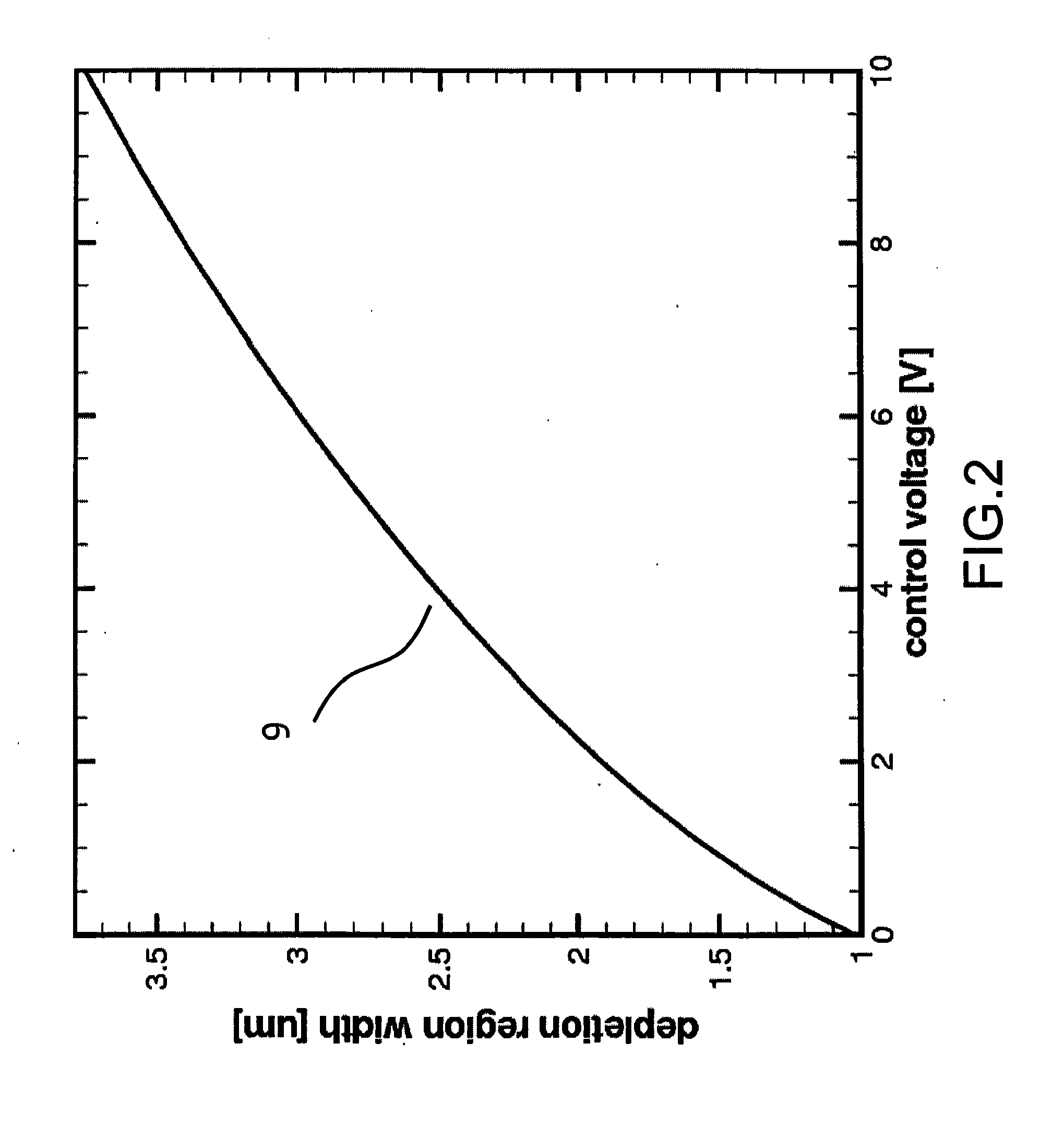
[0102]The plates distance xL can be used to regulate the capacitance values range. The n+ region sh...


PUM

PropertyMeasurementUnit
Timeaaaaaaaaaa
Electrical conductivityaaaaaaaaaa
Electric potential / voltageaaaaaaaaaa

Abstract

A novel semiconductor variable capacitor is presented. The semiconductor structure is simple and is based on a semiconductor variable MOS capacitor structure suitable for integrated circuits, which has at least three terminals, one of which is used to modulate the equivalent capacitor area of the MOS structure by increasing or decreasing its DC voltage with respect to another terminal of the device, in order to change the capacitance over a wide ranges of values. Furthermore, the present invention decouples the AC signal and the DC control voltage avoiding distortion and increasing the performance of the device, such as its control characteristic. The present invention is simple and only slightly dependent on the variations due to the fabrication process. It exhibits a high value of capacitance density and, if opportunely implemented, shows a linear dependence of the capacitance value with respect to the voltage of its control terminal.

Description

BACKGROUND OF THE INVENTION[0001]1. Field of the Invention[0002]The present invention is in the field of semiconductor structures. The present invention is further in the field of semiconductor structures of variable capacitance devices. Particularly, it relates to a MOS type variable capacitance device for semiconductor circuits. The implementation is not limited to a specific technology, and applies to either the invention as an individual component or to inclusion of the present invention within larger systems which may be combined into larger integrated circuits.[0003]2. Brief Description of Related Art[0004]Semiconductor capacitors are one of the fundamental components for integrated circuits. A variable capacitor is a capacitor whose capacitance may be intentionally and repeatedly changed under the influence of DC bias voltages. Variable capacitors are often used in L-C circuits to set the resonance frequency, e.g. to tune a radio (therefore they are sometimes called tuning ca...

Claims


Application Information

Patent Timeline
IPC IPC(8): H01G7/00
CPCH01G7/00Y10T29/435H01L29/94H01L29/93
Inventor MARINO, FABIO ALESSIOMENEGOLI, PAOLO
Owner QUALCOMM INC
Why Eureka
Try Eureka