

Memory Page Buffer
- Summary
- Abstract
- Description
- Claims
- Application Information
AI Technical Summary
Benefits of technology
Problems solved by technology
Method used
Image

Examples
first embodiment
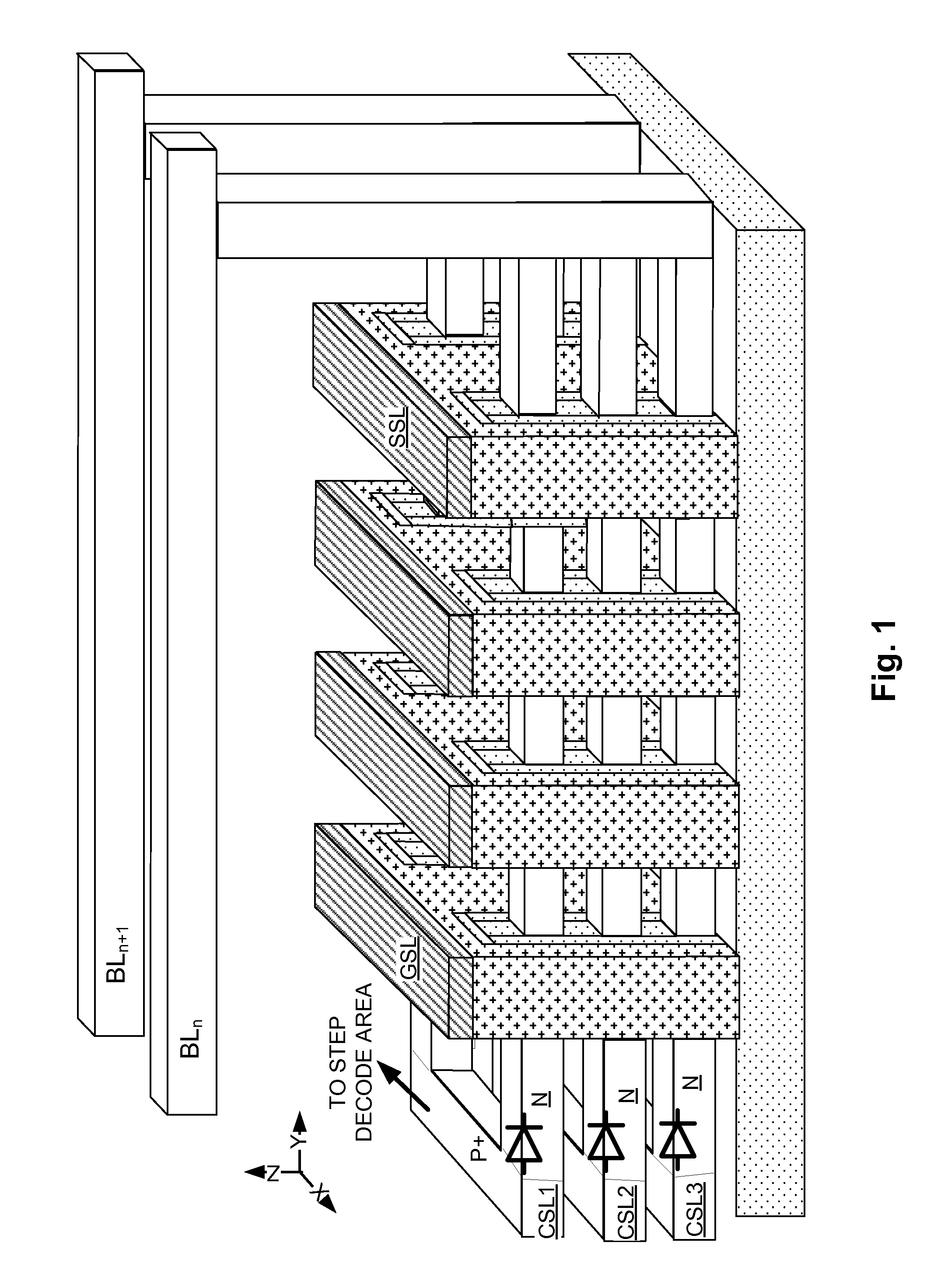
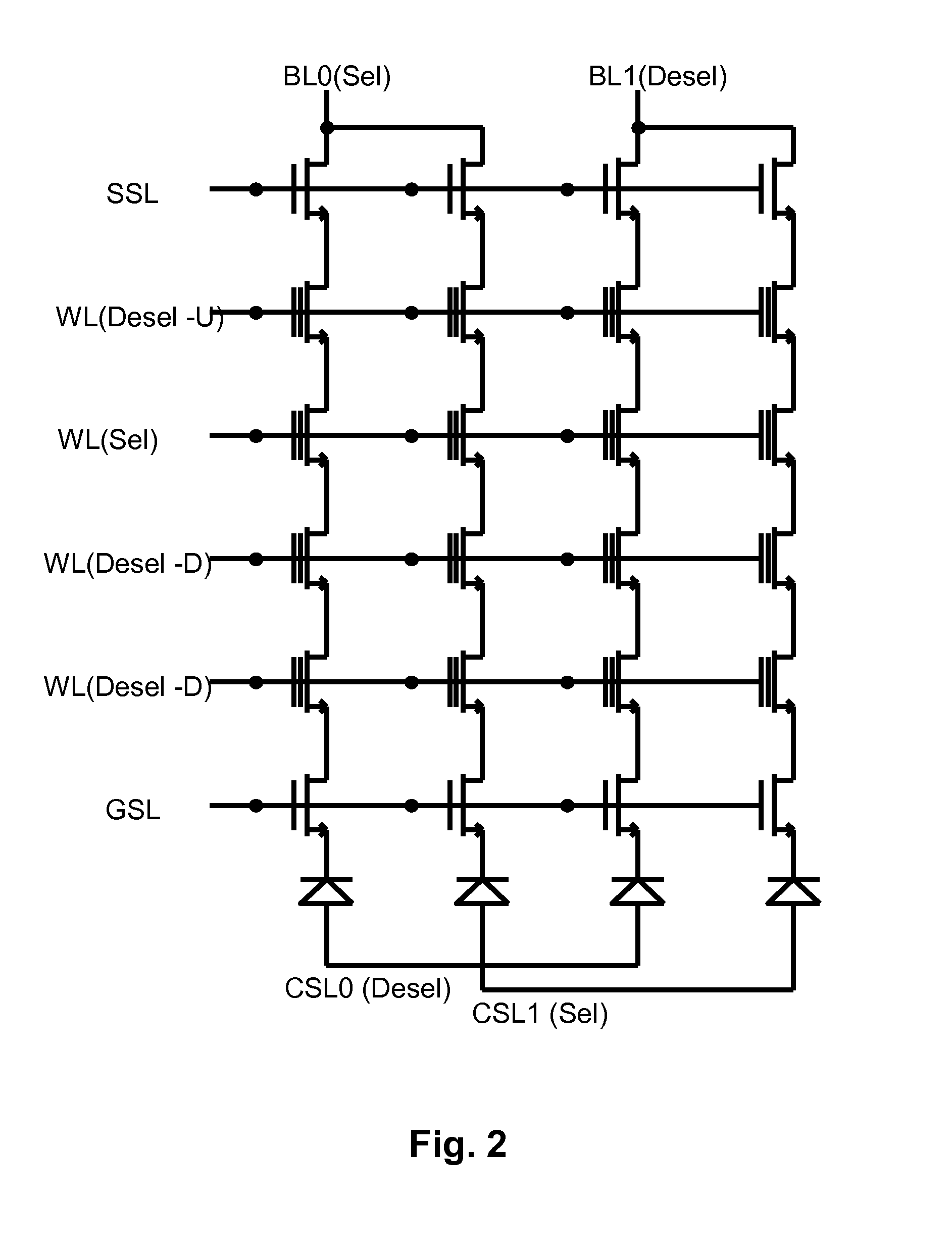
[0082]FIG. 6 is a circuit diagram of a page buffer circuit. The page buffer circuit includes a low voltage sense amplifier and a page buffer logic circuit. Details are shown in further figures and discussion.
second embodiment
[0083]FIG. 7 is a circuit diagram of a page buffer circuit. The page buffer circuit again includes a low voltage sense amplifier and a page buffer logic circuit. Details are shown in further figures and discussion.
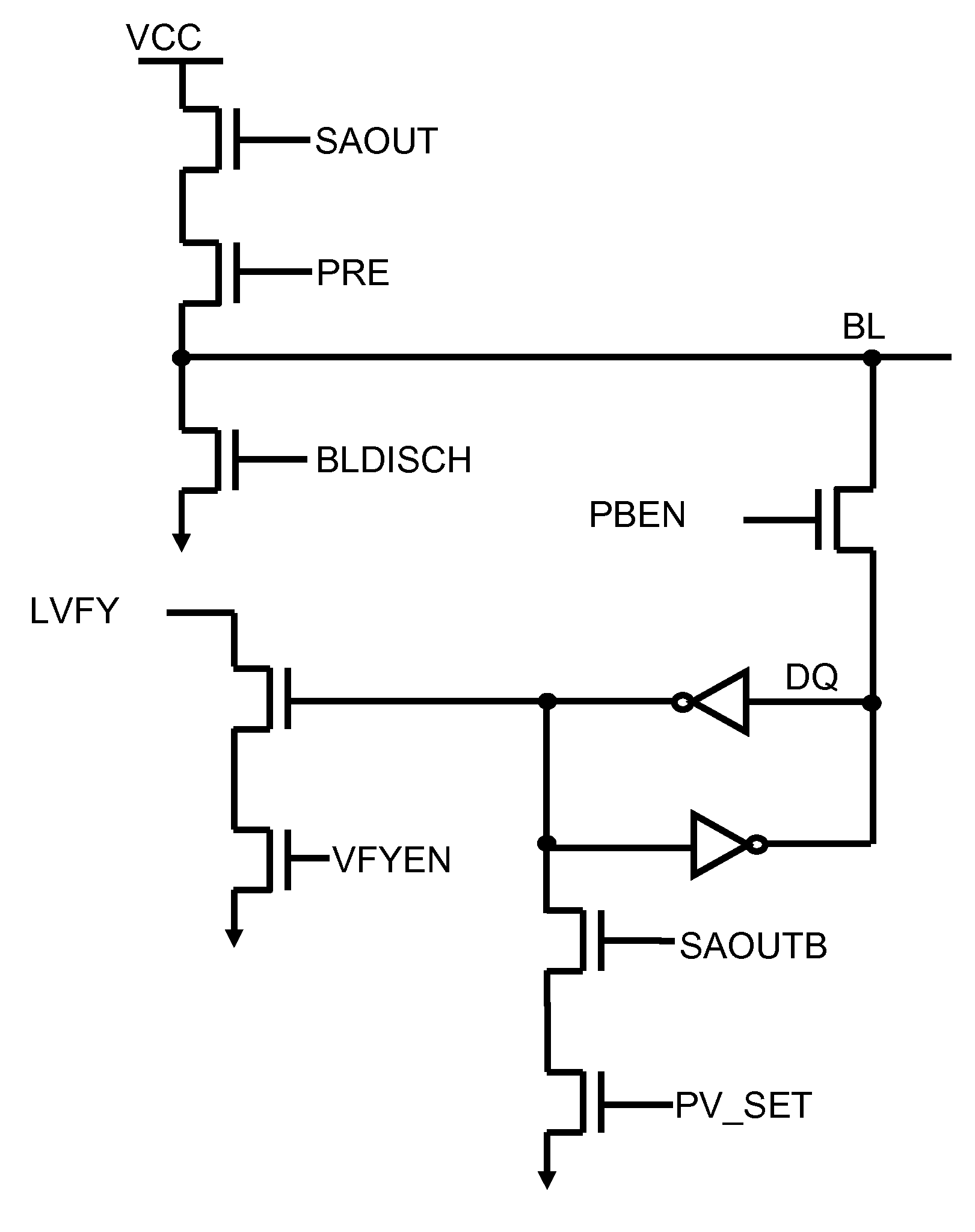
[0084]FIG. 8 is a circuit diagram of a low voltage sensing sense amplifier. The sense amplifier of FIG. 8 is included in the page buffer embodiments shown in FIGS. 6 and 7.
[0085]The low voltage sensing sense amplifier performs differential sensing.
[0086]The sensing node BL is around 100 mV when sensing cells storing “1”. The sensing node BL is around 0V when sensing cells storing “0”.
[0087]The reference REF comes from a stable voltage source and set to 50 mV.
[0088]At first, latch LAT=0 sense amplifier SA latch previous data by M3˜M6
[0089]After bit line BL development, the voltage difference between BL and REF is large enough −50 mV or so—and then the LAT pulse discharges the sense amplifier nodes SAOUT and SAOUTB (trailing B is for bar, two inputs for differential input).
[...
PUM
| Property | Measurement | Unit |
|---|---|---|
| Current | aaaaa | aaaaa |
| Electric potential / voltage | aaaaa | aaaaa |
| Distribution | aaaaa | aaaaa |
Abstract
Description
Claims
Application Information