

Memory circuitry with write boost and write assist
- Summary
- Abstract
- Description
- Claims
- Application Information
AI Technical Summary
Benefits of technology
Problems solved by technology
Method used
Image

Examples
Embodiment Construction
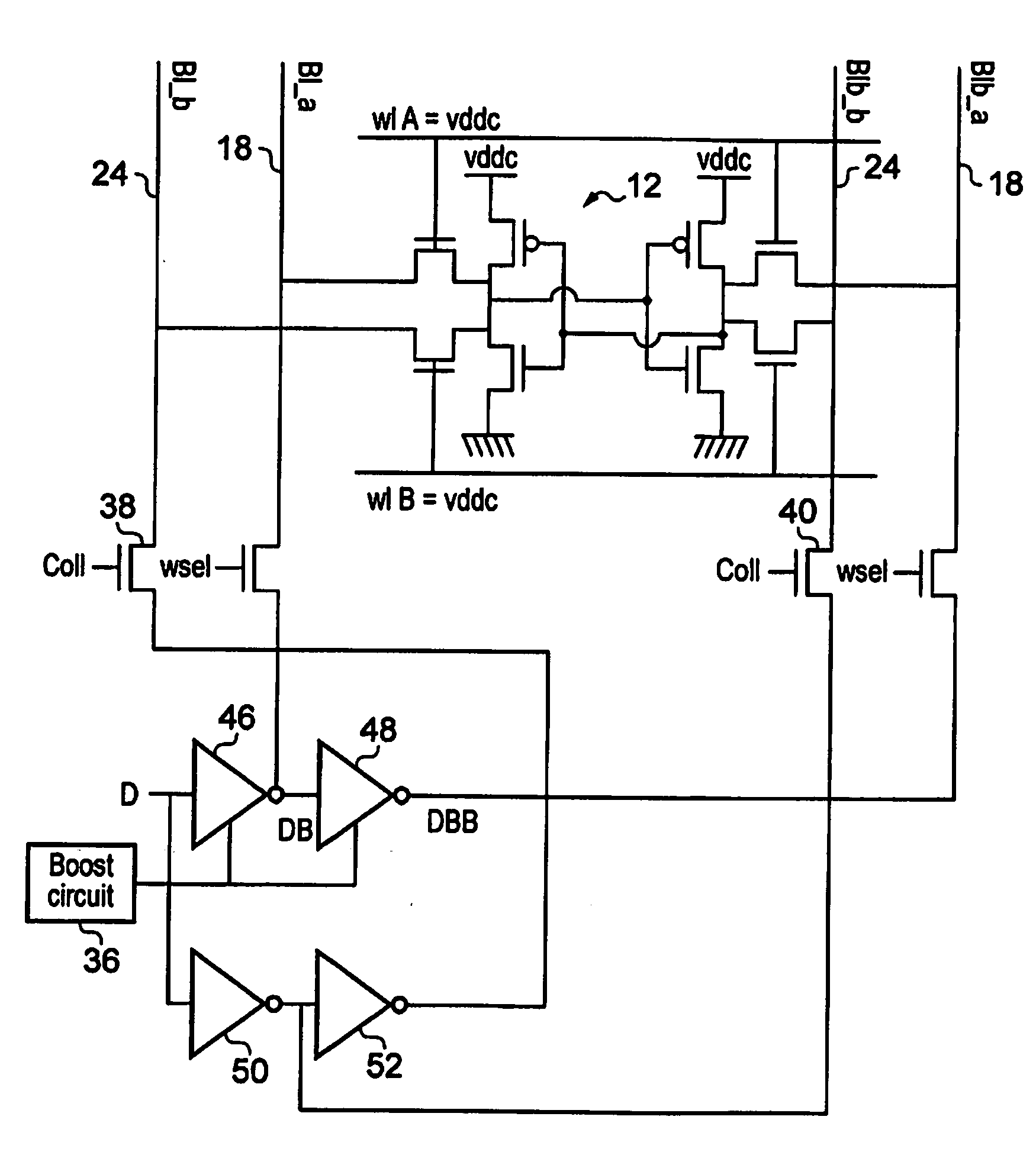
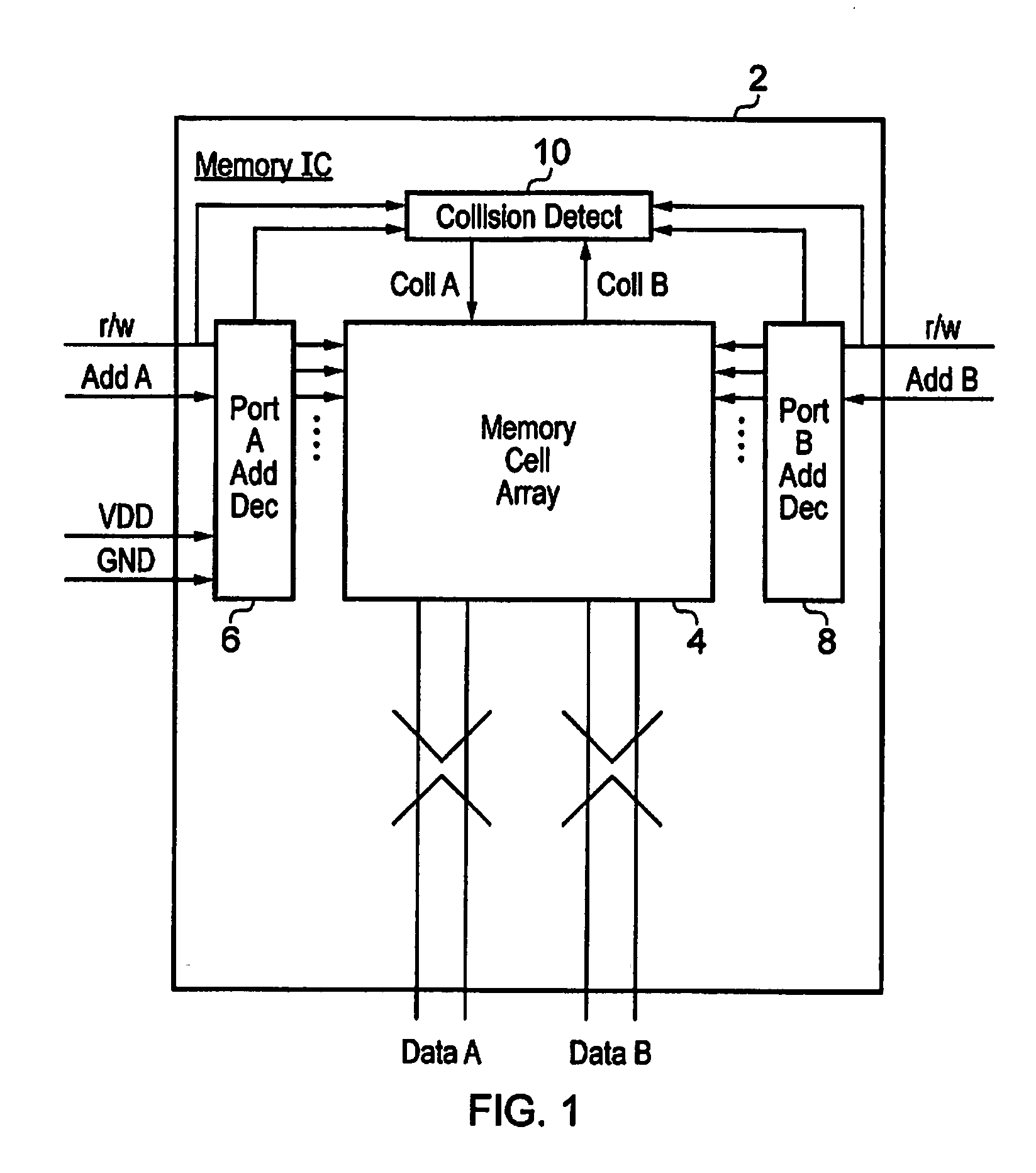
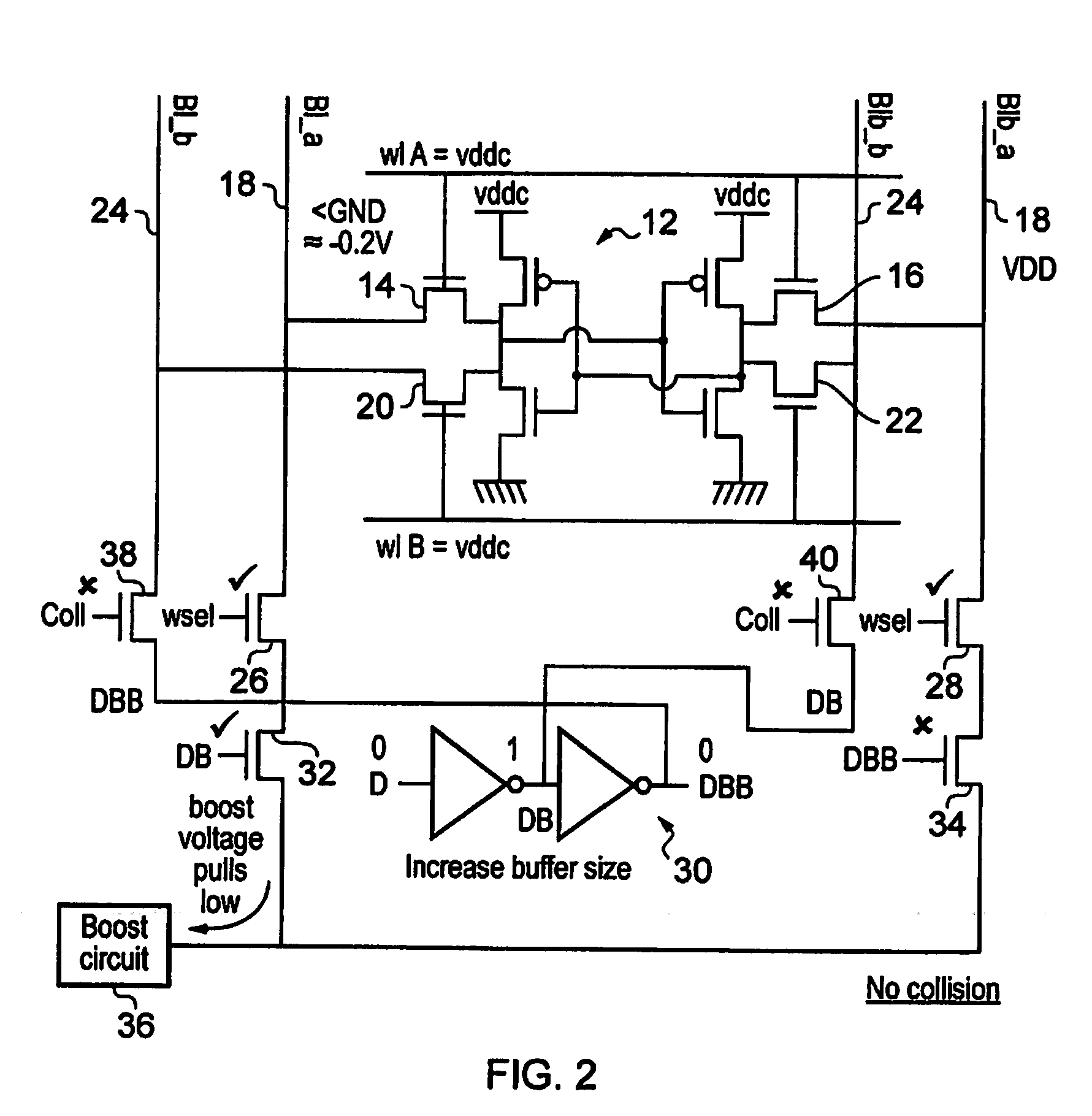
[0040]FIG. 1 schematically illustrates memory circuitry 2 having two data access ports A, B. The present techniques may also be used with memory circuitry having more than two memory access ports. The memory circuitry 2 includes an array of memory cells 4. This array of memory cells comprises a plurality of individual memory cells, such as six transistor (6T) memory cells as will be familiar to those in this technical field. Bit line pairs run through the array of memory cells 4 to provide data access to the memory cells in the form of either read operations or write operations. Separate bit line pairs are provided for port A and port B. Thus, each memory cell will be connected to a bit line pair for port A as well as a bit line pair for port B. Word lines for these respective ports A, B control whether or not the memory cell is coupled to the corresponding bit line pair.
[0041]Memory address decoders 6, 8 are responsive to memory addresses asserted on either port A or port B to asse...
PUM
 Abstract
Description
Claims
Application Information