Polishing head and polishing apparatus
- Summary
- Abstract
- Description
- Claims
- Application Information
AI Technical Summary
Benefits of technology
Problems solved by technology
Method used
Image

Examples
example 1
[0076]First, a p-type, 300 mm diameter silicon single crystal ingot having an orientation of and a resistivity of 8 to 12 Ωcm pulled by the Czochralski method was sliced into thin disk-shaped wafers. Chamfering processes were performed on the outer edges of the wafers to prevent the wafers from being broken and chipped, and lapping processes were then performed to flatten the wafers. Next, etching processes were performed to remove strain by machining remaining on the surfaces of the lapped wafers. Both of the front and back surfaces of the wafers were double-side polished. The chamfered portions were also polished. The thicknesses of the wafers were each adjusted to be 0.775 mm.
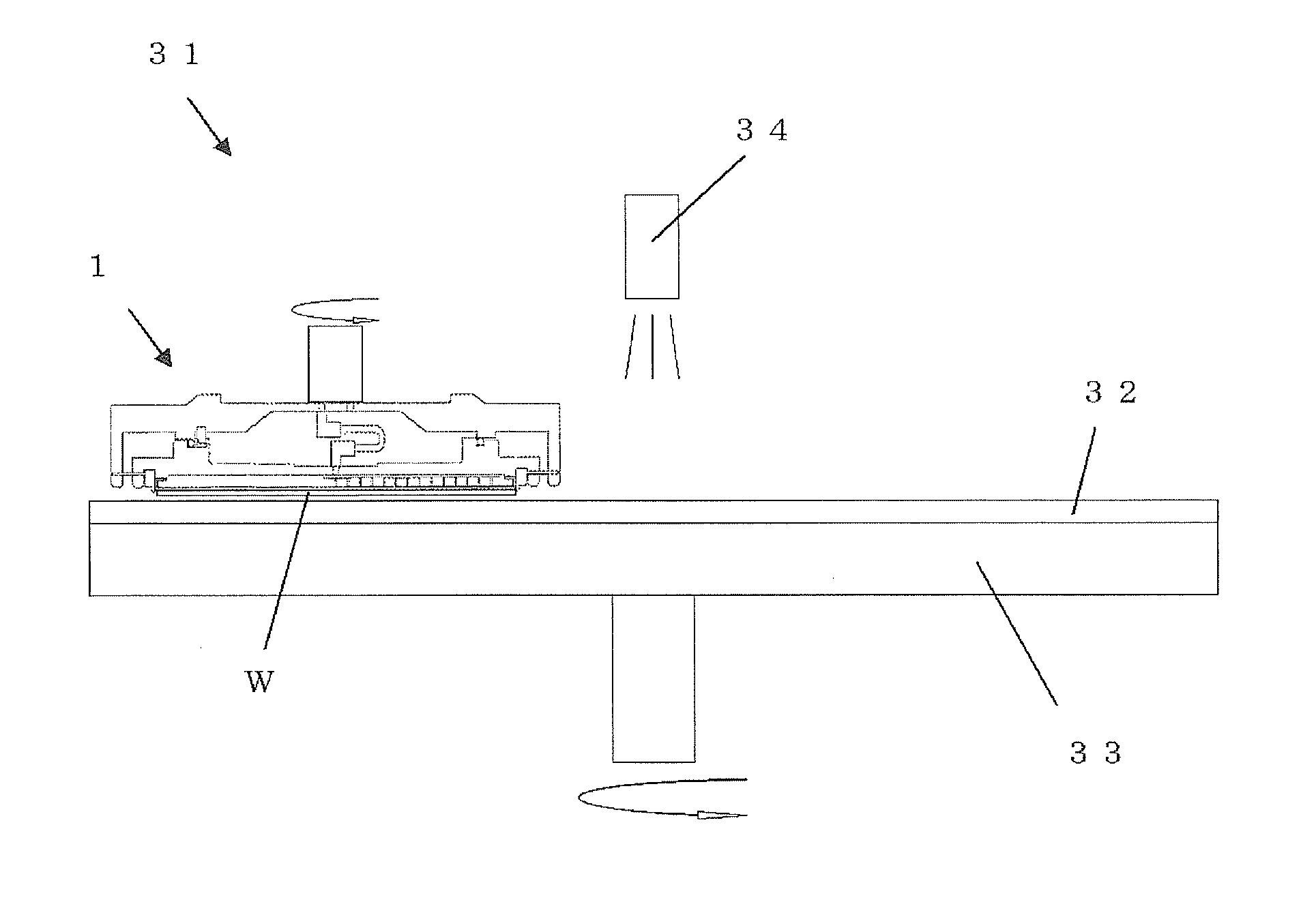
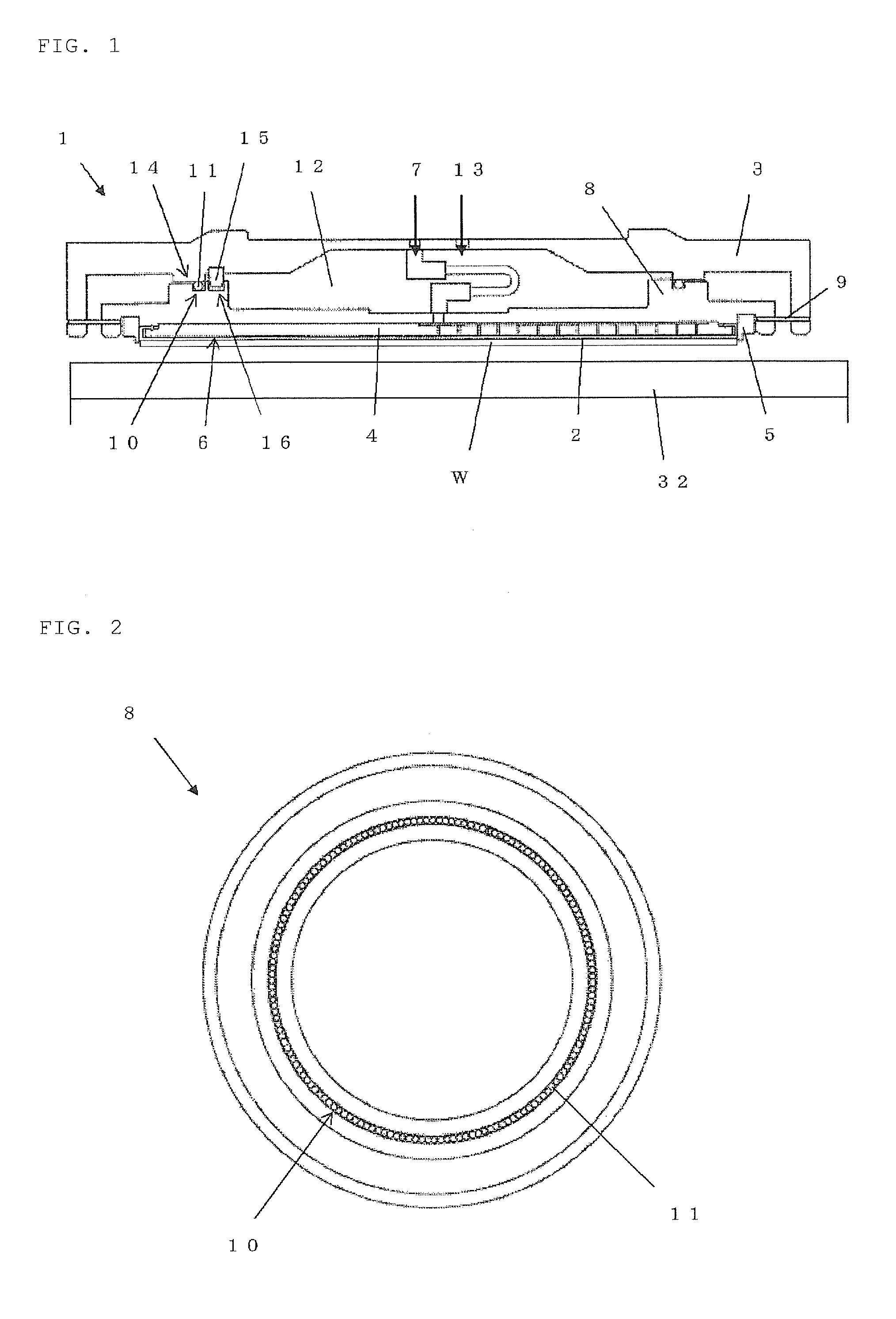
[0077]A silicon wafer was polished with the polishing apparatus of the present invention shown in FIG. 4, including the polishing head of the present invention shown in FIG. 1. The used polishing head was configured as follows: a boot-shaped rubber film made of silicone 70° having a thickness of 1 mm, a low...
example 2
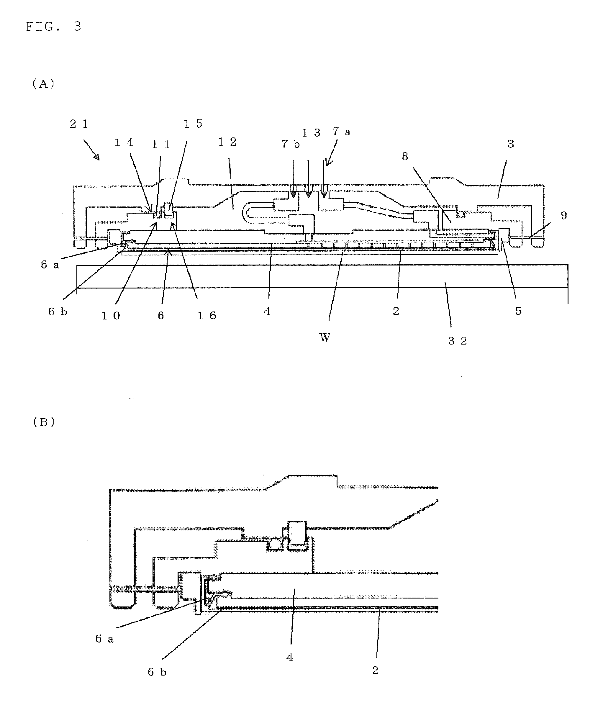
[0091]The rough polishing and final polishing were consecutively performed on silicon wafers as with Example 1 with the polishing head of the present invention including the first sealed space portion divided into two sealed spaces, shown in FIG. 3 and the polishing apparatus of the present invention, shown in FIG. 4. After cleaning, the same evaluation as Example 1 was carried out.
[0092]Polishing conditions and so on will be described below.
[0093]A polishing pad of a polyester nonwoven fabric including urethane resin (an ASKER C hardness of 60°) was used. A 10.5 pH alkali solution containing colloidal silica was used as a polishing slurry. The polishing head and the turn table were each rotated at 30 rpm. The polishing pressure to the front surface of the wafer was set to 15 kPa and the polishing pressure to its side wall face was 17 kPa for the rough polishing. The polishing time was three minutes and two stage polishing was performed.
[0094]A suede type polishing pad (an ASKER C h...
PUM
 Abstract
Description
Claims
Application Information