Eureka AIR delivers breakthrough ideas for toughest innovation challenges, trusted by R&D personnel around the world.

Method for Manufacturing Insulating Film and Method for Manufacturing Semiconductor Device

Inactive Publication Date: 2008-08-28
SEMICON ENERGY LAB CO LTD
View PDF25 Cites 2 Cited by
  • Summary
  • Abstract
  • Description
  • Claims
  • Application Information

AI Technical Summary

Benefits of technology

[0014]As the organic solvent used for the etching, medium alcohol in which the carbon number is in the range of 3 to 5, such as butanol or propanol is preferable. By using the above-described alcohol as an etchant, the etching rate suitable for etching and high selection ratio with respect to a mask can be obtained when wet etching is performed on the thin film which has been hardened by baking. Further, by using such an organic solvent as an etchant, unlike the case where an inorganic material such as hydrofluoric acid is used as an etchant, roughness of the surface of a conductive film such as a wiring, an electrode, or the like under the insulating layer can be suppressed and the risk for handling can be reduced.
[0018]According to the method for manufacturing an insulating film of the present invention, since wet etching can be used, the taper angle in edge of a patterned insulating film can be suppressed to be small and an insulating film having higher flatness can be formed. Further, according to the method for manufacturing an insulating film of the present invention, a problem in that the hygroscopicity of an insulating film is increased by increase of OH radicals does not occur unlike the case of dry etching. Furthermore, since an insulating film can be formed of a conventional non-photosensitive siloxane resin, an inexpensive raw material can be used.
[0019]Further, according to the method for manufacturing a semiconductor device of the present invention, in which the above-described manufacturing method of an insulating film is used, by suppressing the taper angle in the edge of an insulating film to be small, extremely thinning or disconnecting a wiring or a film in the edge of the insulating film, formed to be in contact with the insulating film can be prevented. Therefore, the yield and / or reliability of a semiconductor device can be increased. Further, in the case of a semiconductor device having a light-emitting element, by suppressing the taper angle in the edge of an insulating film to be small, an electroluminescent layer can be prevented from being partially thinning extremely or disconnecting due to a step. Therefore, the reliability of a light-emitting element, and then the reliability of a semiconductor device having the light-emitting element can be improved.
[0020]Further, according to the method for manufacturing a semiconductor device of the present invention, in which the above-described manufacturing method of an insulating film is used, since the problem in that hygroscopicity of an insulating film is increased by increase of OH radicals does not occur unlike the case of dry etching, the reliability of a light-emitting element and then the reliability of a semiconductor device can be prevented from being adversely affected by moisture in the insulating film. In addition, in the case of a semiconductor device having a light-emitting element, the deterioration of the light-emitting element can be suppressed by suppressing the hygroscopicity of an insulating film, whereby the reliability of the semiconductor device can be improved.
[0021]Furthermore, according to the method for manufacturing a semiconductor device of the present invention, in which the above-described manufacturing method of an insulating film is used, since the insulating film can be formed of a conventional non-photosensitive siloxane resin, an inexpensive raw material can be used, whereby the manufacturing cost of the semiconductor device can be suppressed.

Problems solved by technology

However, in the case where an insulating film formed of a siloxane resin is patterned by dry etching, the taper angle of a cross-sectional surface tends to be large.
If the taper angle is large, in an edge of the insulating film formed of a siloxane resin, a problem such as extreme thinning or disconnecting of a wiring or a film formed to be in contact with the insulating film tends to occur.
If an insulating film does not have sufficiently high flatness, the electrode of the light-emitting element formed over the insulating film has roughness, and a problem of locally and extremely thinning, disconnecting due to a step, or the like of the electroluminescent layer formed over the electrode tends to occur.
Further, deterioration of the electroluminescence material tends to be increased in the extremely thin portion of the electroluminescent layer, which causes reduction of reliability of the light-emitting element.
Further, since the pair of electrodes is short-circuited in a portion where the electroluminescent layer is disconnected due to a step, the light-emitting element does not emit light or deterioration of the electroluminescence material tends to be increased from the periphery of the short-circuited portion, which causes reduction of reliability of the light-emitting element.
In addition, when the insulating film formed of a siloxane resin is patterned by dry etching, there is also a problem in that OH radicals tend to be generated on the surface of the insulating film formed of a siloxane resin by plasma generated at the time of etching.
If OH radicals are increased, the hygroscopicity of the insulating film is increased and moisture in the insulating film may adversely affect the reliability of a semiconductor element.
In particular, the deterioration of the electroluminescence material used in the above-described light-emitting element is increased by moisture.
Therefore, the degree of hygroscopicity in the insulating film is a big issue by which the reliability of a semiconductor device is determined.
However, the siloxane resin having photosensitivity is currently under development for various uses, and inexpensive products thereof have not penetrated the market yet.

Method used


Image

  • Method for Manufacturing Insulating Film and Method for Manufacturing Semiconductor Device
  • Method for Manufacturing Insulating Film and Method for Manufacturing Semiconductor Device
  • Method for Manufacturing Insulating Film and Method for Manufacturing Semiconductor Device

Examples


embodiment mode 1

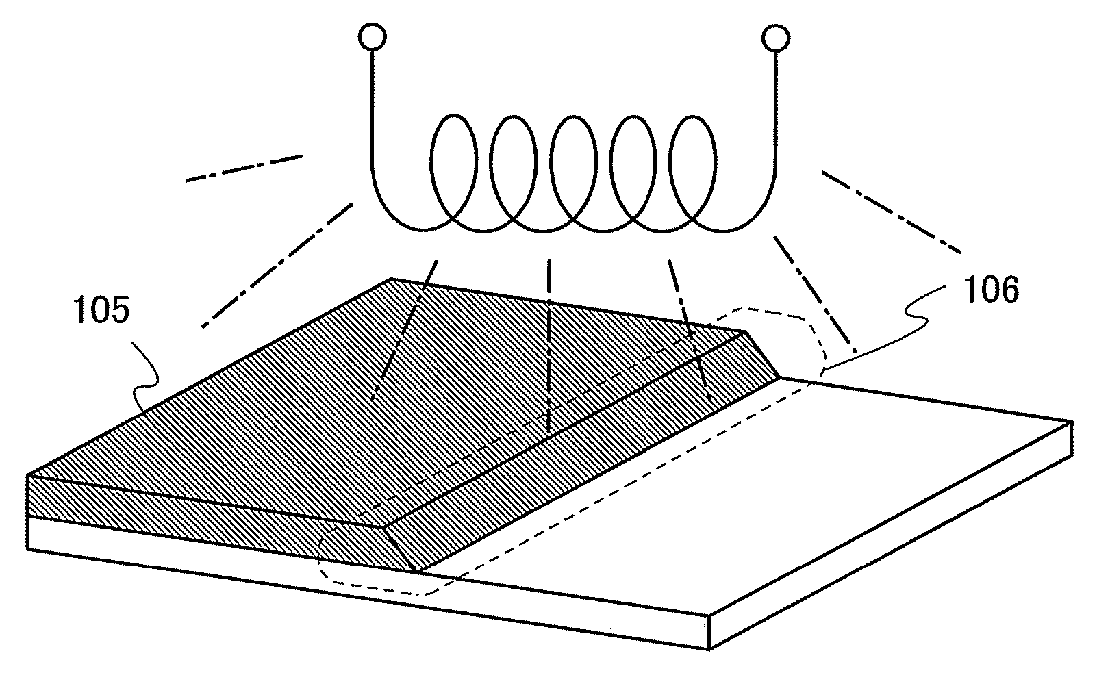
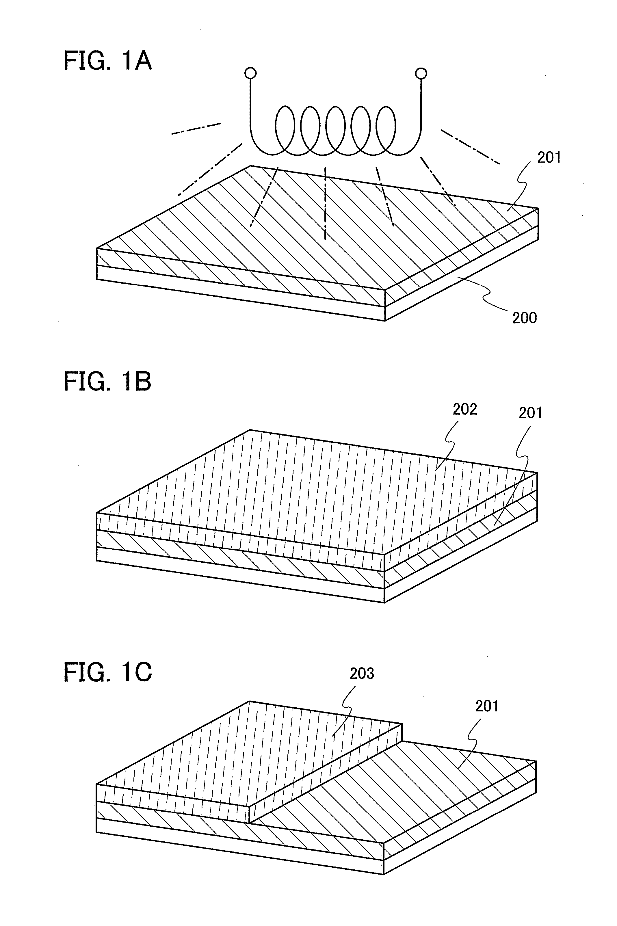
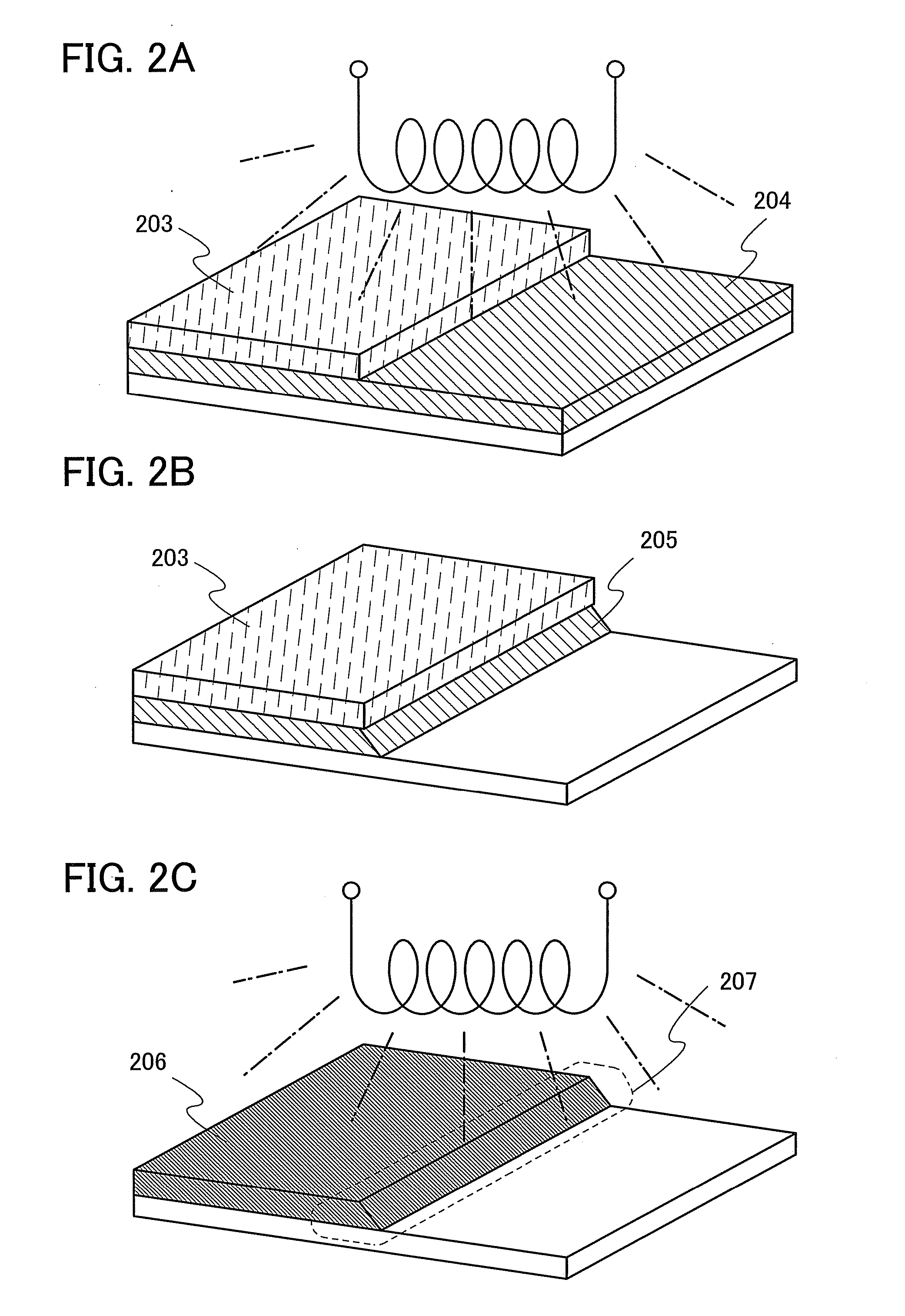
[0042]In this embodiment mode, a method for manufacturing an insulating film of the present invention in which a photolithography method is used is described using FIGS. 1A to 1C and 2A to 2C. First, as shown in FIG. 1A, a suspension in which a siloxane resin or a siloxane-based material which is a precursor of a siloxane resin is dispersed is applied over a substrate 200, to form a thin film 201. Siloxane resin is a material in which a skeleton structure is constructed by the bond of silicon (Si) and oxygen (O). As a substituent, at least one kind selected from fluorine, a fluoro group, an organic group (e.g., an alkyl group or an aromatic hydrocarbon) may be used in addition to hydrogen.

[0043]A solvent of the suspension is preferably an organic solvent into which a siloxane resin or a siloxane-based material can be dispersed; for example, propylene glycol monomethyl ether acetate (PGMEA), 3-methoxy-3-methyl-1-butanol (MMB), N-methyl-2-pyrrolidone (NMP), or the like can be used. In...

embodiment mode 2

[0070]In this embodiment mode, a method for manufacturing an insulating film of the present invention is described using FIGS. 3A to 3C and 4A to 4C. First, as shown in FIG. 3A, similarly to Embodiment Mode 1, a suspension in which a siloxane resin or a siloxane-based material which is a precursor of a siloxane resin is dispersed is applied over a substrate 100, to form a thin film 101. Siloxane resin is a material in which a skeleton structure is constructed by the bond of silicon (Si) and oxygen (O). As a substituent, at least one kind selected from fluorine, a fluoro group, an organic group (e.g., an alkyl group or an aromatic hydrocarbon) may be used other than hydrogen.

[0071]A solvent of the suspension is preferably an organic solvent into which a siloxane resin or a siloxane-based material can be dispersed; for example, propylene glycol monomethyl ether acetate (PGMEA), 3-methoxy-3-methyl-1-butanol (MMB), N-methyl-2-pyrrolidone (NMP), or the like can be used. In this embodimen...

embodiment mode 3

[0085]Next, a specific method for manufacturing a semiconductor device of the present invention is described. Note that the case where a light-emitting element and a transistor are manufactured over the same substrate is given as an example for description in this embodiment mode.

[0086]First, as shown in FIG. 5A, an insulating film 301 is formed over a substrate 300. As the substrate 300, for example, a glass substrate made of barium-borosilicate glass or alumino-borosilicate glass, a quartz substrate, a ceramic substrate, or the like can be used. Further, a metal substrate such as a stainless-steel substrate or a substrate in which an insulating film is formed on the surface of a silicon substrate may be used as well. A substrate made of a synthetic resin having flexibility such as plastics which generally has the heat-resistance temperature which is lower than those of the above-described substrates can be used as long as it can withstand the process temperature in a manufacturing...


PUM


Abstract

A method for manufacturing an insulating film, by which the insulating film can be formed of a non-photosensitive siloxane resin and formed into a desired shape by wet etching. A thin film is formed with a suspension in which a siloxane resin or a siloxane-based material is included in an organic solvent; a first heat treatment is performed on the thin film; a mask is formed over the thin film after the first heat treatment; wet etching with an organic solvent is performed to process the shape of the thin film after the first heat treatment; and a second heat treatment is performed on the processed thin film.

Description

BACKGROUND OF THE INVENTION[0001]1. Field of the Invention[0002]The present invention relates to a method for manufacturing an insulating film processed into a desired shape. In addition, the present invention relates to a method for manufacturing a semiconductor device in which the insulating film is used as an interlayer film.[0003]2. Description of the Related Art[0004]As for an insulating film provided in a semiconductor element or between wirings, it is important to have, in addition to low permittivity, flatness on its surface in order to uniformly perform photolithography or etching of each film formed over the insulating film or improve coverage with each film in a step of the insulating film. In the point of surface flatness, a higher quality insulating film can be formed easily by a coating method (SOD: Spin On Deposition) rather than by a CVD method. In particular, an insulating film formed of a siloxane resin by a coating method has been widely used as an insulating film...

Claims


Application Information

Patent Timeline
IPC IPC(8): H01L21/311
CPCH01L21/02126H01L21/02216H01L27/3295H01L21/31133H01L21/3122H01L21/02282H10K59/122H01L21/31
Inventor FUJII, TERUYUKI
Owner SEMICON ENERGY LAB CO LTD
Why Eureka
Eureka Blog
Learn More