Organic layer deposition apparatus and method of manufacturing organic light-emitting display device by using the same

a technology of organic layer and deposition apparatus, which is applied in the direction of spray nozzles, coatings, vacuum evaporation coatings, etc., can solve the problems of difficult to achieve high light-emission efficiency with such a structure, difficult to pattern fine organic thin films, emission layer, etc., to achieve easy manufacturing, simple application, the effect of improving manufacturing yield and deposition efficiency

Active Publication Date: 2012-11-29
SAMSUNG DISPLAY CO LTD
View PDF6 Cites 34 Cited by
  • Summary
  • Abstract
  • Description
  • Claims
  • Application Information

AI Technical Summary

Benefits of technology

[0009]According to aspects of embodiments of the present invention, an organic layer deposition apparatus may be easily manufactured, may be simply applied to manufacture large-sized display devices on a mass scale, and improves manufacturing yield and deposition efficiency. According to another aspect of embodiments of the present invention, a method of manufacturing an organic light-emitting display device uses the organic layer deposition apparatus.

Problems solved by technology

However, it is difficult to achieve high light-emission efficiency with such a structure, and thus intermediate layers, including an electron injection layer, an electron transport layer, a hole transport layer, a hole injection layer, or the like, may be additionally interposed between the emission layer and each of the electrodes.
However, it is very difficult to pattern fine patterns of organic thin films such as the emission layer and the intermediate layers, and light-emission efficiencies of red, green, and blue lights vary depending on the layers.
Thus, it is difficult to perform the patterning operation on a large-sized substrate by using the conventional organic layer deposition apparatus.
Therefore, a large-sized organic light-emitting display device having satisfactory driving voltage, current density, brightness, color purity, light-emission efficiency, and lifespan may not be manufactured.

Method used


Image

  • Organic layer deposition apparatus and method of manufacturing organic light-emitting display device by using the same
  • Organic layer deposition apparatus and method of manufacturing organic light-emitting display device by using the same
  • Organic layer deposition apparatus and method of manufacturing organic light-emitting display device by using the same

Examples


Embodiment Construction

[0059]Some exemplary embodiments of the present invention will be described more fully hereinafter with reference to the accompanying drawings; however, embodiments of the present invention may be embodied in different forms and should not be construed as limited to the exemplary embodiments illustrated and set forth herein. Rather, these exemplary embodiments are provided by way of example for understanding of the invention and to convey the scope of the invention to those skilled in the art. As those skilled in the art would realize, the described embodiments may be modified in various ways, all without departing from the spirit or scope of the present invention.

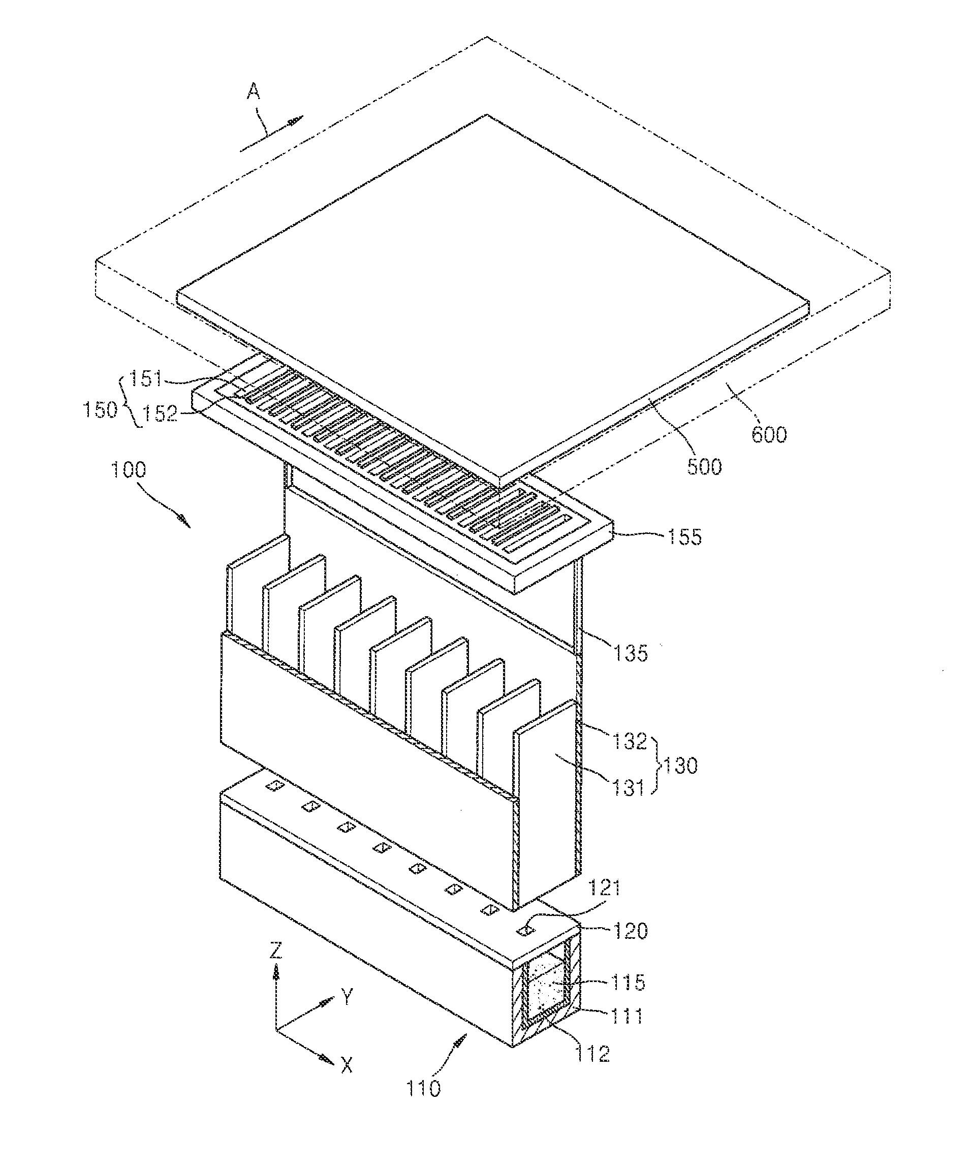
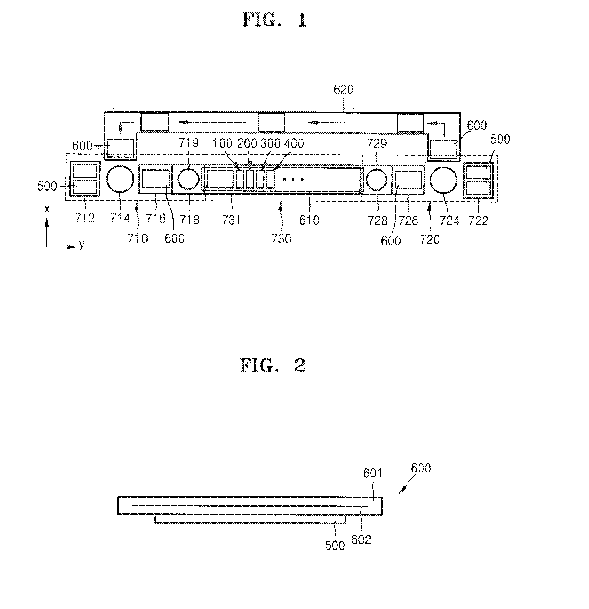
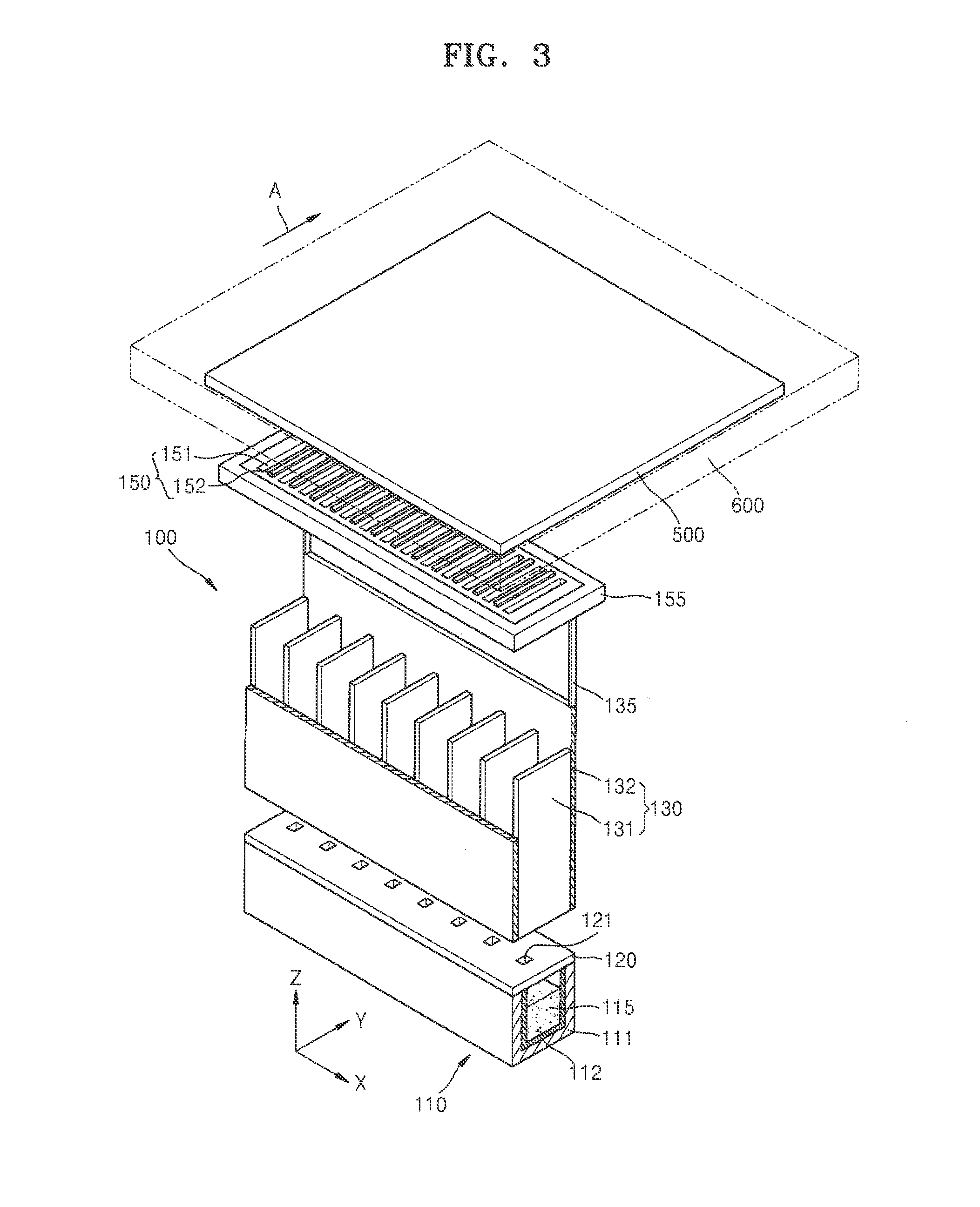
[0060]FIG. 1 is a schematic block diagram of an organic layer deposition apparatus according to an embodiment of the present invention;

[0061]Referring to FIG. 1, the organic layer deposition apparatus according to an embodiment of the present invention includes a loading unit 710, a deposition unit 730, an unloading unit 7...


PUM

PropertyMeasurementUnit
thicknessaaaaaaaaaa
thicknessaaaaaaaaaa
distanceaaaaaaaaaa

Abstract

An organic layer deposition apparatus for forming an organic layer on a substrate includes: a deposition source configured to discharge a deposition material; a deposition source nozzle unit arranged at a side of the deposition source and including a plurality of deposition source nozzles; and a patterning slit sheet facing the deposition source nozzle unit and including a plurality of patterning slits and at least one spacer arranged between a pair of adjacent patterning slits of the plurality of patterning slits, the patterning slit sheet being smaller than the substrate in at least one of a first direction or a second direction perpendicular to the first direction, and the substrate is spaced apart from the organic layer deposition apparatus by a predetermined distance, and at least one of the substrate or the organic layer deposition apparatus is movable relative to the other.

Description

CROSS-REFERENCE TO RELATED APPLICATION[0001]This application claims priority to and the benefit of Korean Patent Application No. 10-2011-0049792, filed on May 25, 2011 in the Korean Intellectual Property Office, the entire content of which is incorporated herein by reference.BACKGROUND[0002]1. Field[0003]Aspects of embodiments of the present invention relate to an organic layer deposition apparatus and a method of manufacturing an organic light-emitting display device by using the same.[0004]2. Description of the Related Art[0005]Organic light-emitting display devices typically have a larger viewing angle, better contrast characteristics, and a faster response rate than other display devices, and thus have drawn attention as a next-generation display device.[0006]Organic light-emitting display devices generally have a stacked structure including an anode, a cathode, and an emission layer interposed between the anode and the cathode. The devices display images in color when holes and...

Claims


Application Information

Patent Timeline
Patent Type & Authority Applications(United States)
IPC IPC(8): H01L33/08B05C13/00B05C21/00B05B1/00
CPCC23C14/042C23C14/243C23C14/12H10K71/166H10K71/00C23C14/04
Inventor LEE, DONG-KYUKIM, MU-HYUNSONG, YOUNG-ROKLEE, SANG-PILSONG, JUNG-BAEKIM, JONG-HEONKIM, BYUNG-SULEE, YUN-MIRYU, JAE-KWANG
Owner SAMSUNG DISPLAY CO LTD
Why Eureka
Try Eureka