Method for manufacturing epitaxial crystal substrate, epitaxial crystal substrate and semiconductor device

a technology of epitaxial crystal substrates and crystal substrates, which is applied in the direction of polycrystalline material growth, crystal growth process, chemically reactive gases, etc., can solve the problems of preventing the production of high-performance devices and degrading crystallinity, and achieves the prevention of poor crystallinity of epitaxial layers due to lattice mismatch, and the growth of high-quality epitaxial layers in a short tim

Active Publication Date: 2012-11-29
JX NIPPON MINING& METALS CORP
View PDF1 Cites 1 Cited by
  • Summary
  • Abstract
  • Description
  • Claims
  • Application Information

AI Technical Summary

Benefits of technology

[0045]According to the present invention, since poor crystallinity of an epitaxial layer due to lattice mismatch can be prevented during growth of an epitaxial layer of a semiconductor having a lattice constant different from that of a substrate, the resulting epitaxial crystal substrate can have a uniform high-quality epitaxial layer. Since a composition modulation layer formed on the substrate is much thinner than conventional composition gradient layers, the layer can be grown within a short time at low manufacturing cost.

Problems solved by technology

The misfit dislocation induced in the epitaxial layer degrades crystallinity in the epitaxial layer and precludes production of a high-performance device.

Method used


Image

  • Method for manufacturing epitaxial crystal substrate, epitaxial crystal substrate and semiconductor device
  • Method for manufacturing epitaxial crystal substrate, epitaxial crystal substrate and semiconductor device
  • Method for manufacturing epitaxial crystal substrate, epitaxial crystal substrate and semiconductor device

Examples


Embodiment Construction

[0053]An embodiment of the present invention will be described with reference to attached drawings below.

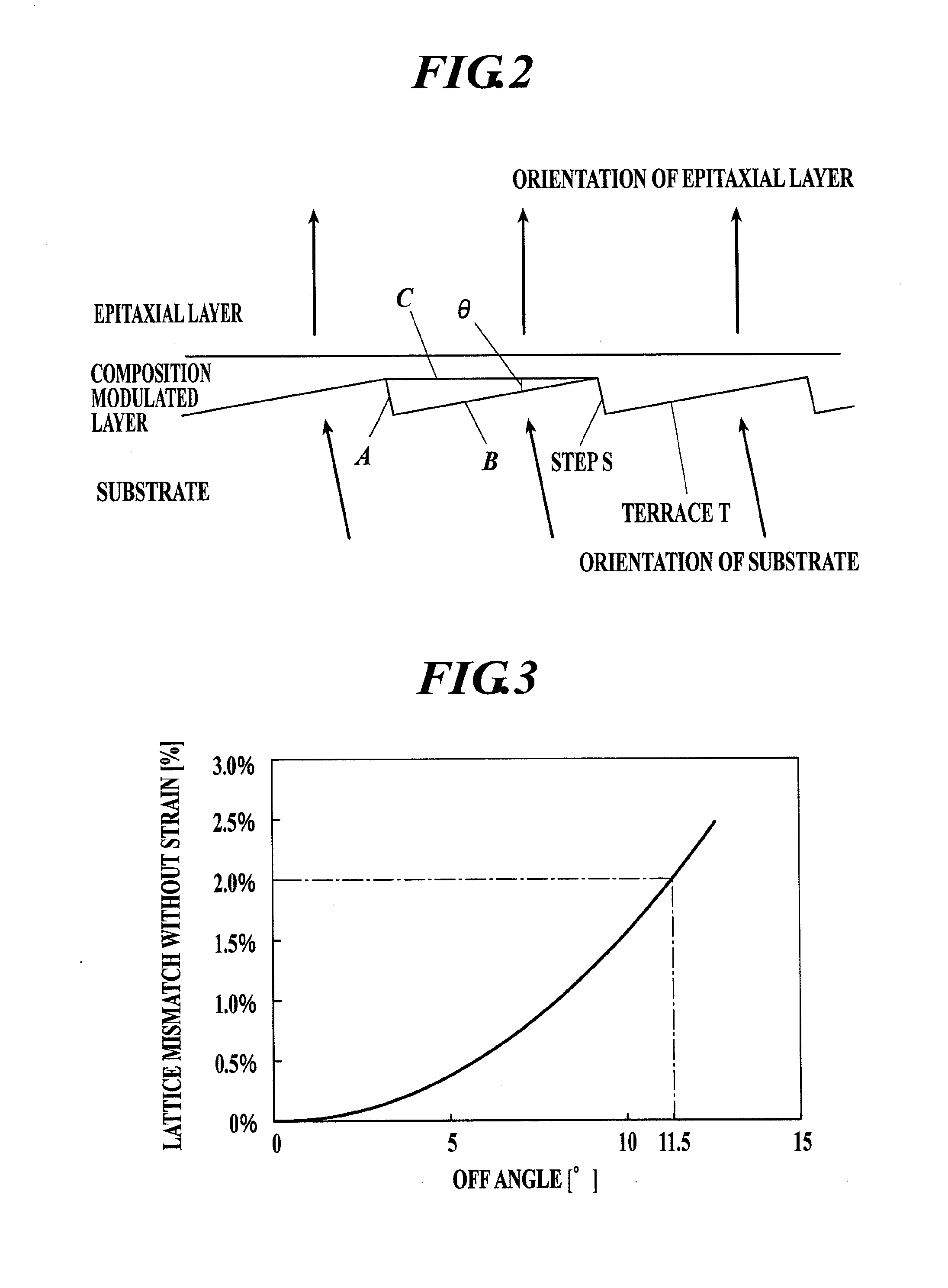
[0054]In the embodiment, a composition modulation layer of InxGa1-xAs (0≦x≦1) is formed on an InP substrate and an epitaxial layer of InAsyP1-y (y=0.12) is grown thereon by MOCVD.

[0055]Since InP and InAs0.12P0.88 have respectively lattice constants of 5.86 Å and 5.883 Å, their lattice mismatch is as large as 0.39%. Hence, an epitaxial layer of InAs0.12P0.88 grown directly on the InP substrate has poor crystallinity. In the embodiment, a composition modulation layer of InxGa1-xAs (0≦x≦1) is formed on the InP substrate, so that poor crystallinity, which is caused by dislocation due to lattice mismatch, can be prevented in the epitaxial layer of InAs0.12P0.88.

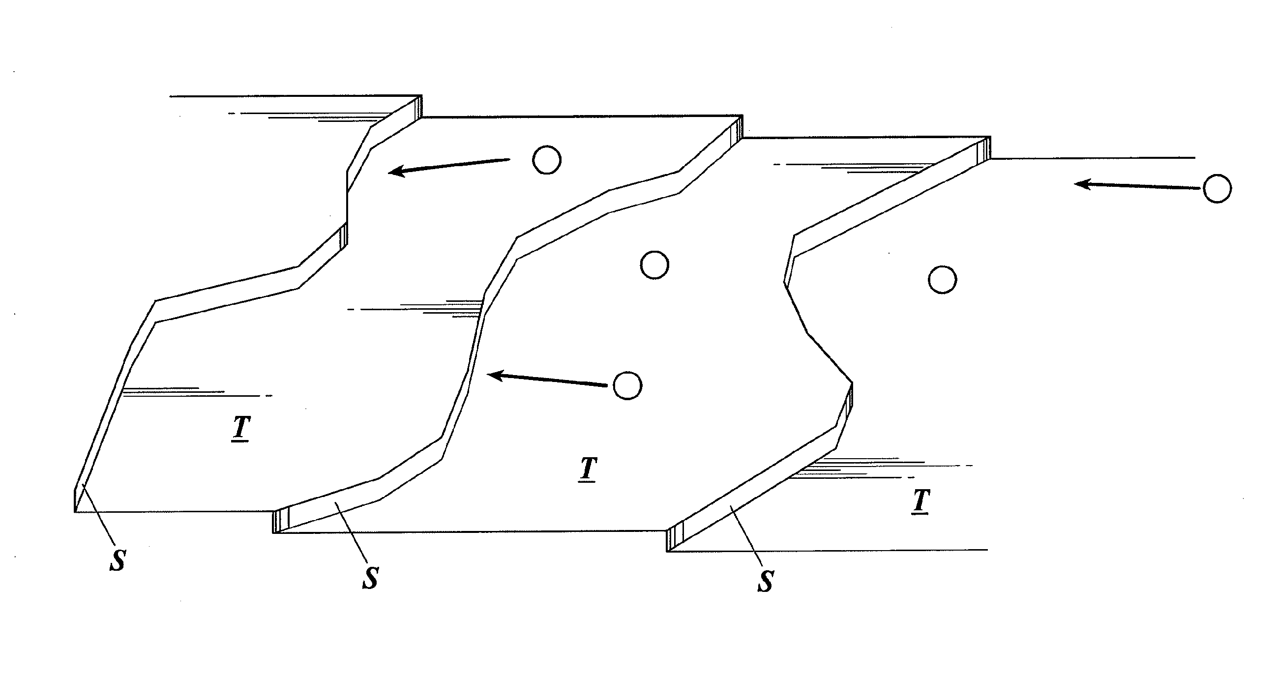
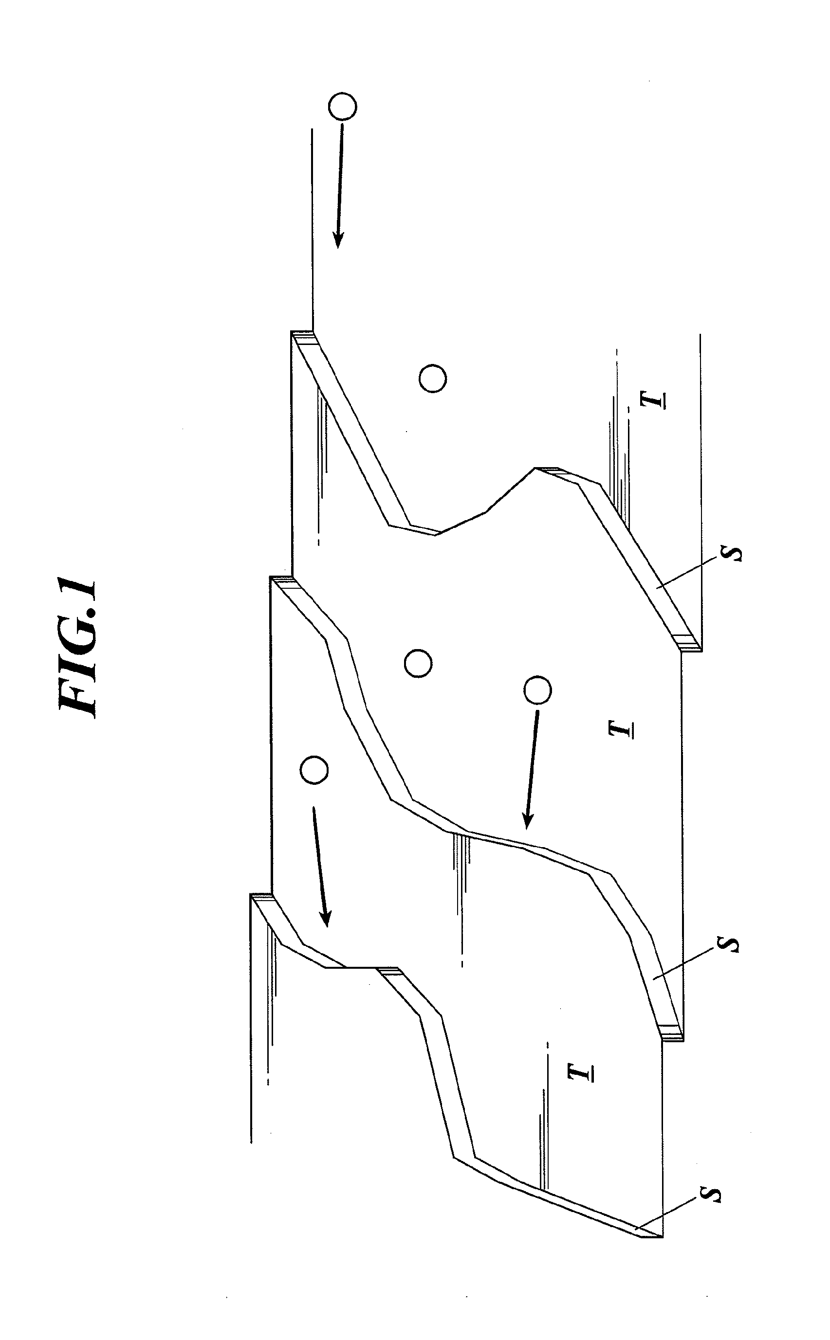
[0056]An InP substrate is prepared which has orientation tilting at a slight off angle θ from a predetermined orientation (for example, (1 0 0)). Here, the off angle of the substrate is determined in view of a lattice mismatch ...


PUM

PropertyMeasurementUnit
light wavelengthaaaaaaaaaa
temperatureaaaaaaaaaa
thicknessaaaaaaaaaa

Abstract

Disclosed is a technology of manufacturing, at low cost, an epitaxial crystal substrate provided with a high-quality and uniform epitaxial layer, said technology being useful in the case of growing the epitaxial layer composed of a semiconductor having a lattice constant different from that of the substrate. The substrate, which is composed of a first compound semiconductor, and which has a step-terrace structure on the surface, is used, and on the surface of the substrate, a composition modulation layer composed of a second compound semiconductor is grown by step-flow, while changing the composition in the same terrace. Then, the epitaxial crystal substrate is manufactured by growing, on the composition modulation layer, the epitaxial layer composed of the third compound semiconductor having the lattice constant different from that of the first compound semiconductor.

Description

TECHNICAL FIELD[0001]The present invention relates to a method for manufacturing an epitaxial crystal substrate used in manufacturing a semiconductor device and in particular to a technique effective for an epitaxial layer that is not lattice-matched with a substrate.BACKGROUND ART[0002]In recent years, semiconductor devices used in laser diodes or light receiving elements have been put to practical use over a wide light wavelength range from near infrared to blue.[0003]Substrates used in these semiconductor devices are usually manufactured by epitaxial growth. It has been well known that heterojunctions for connection of different materials are used in these substrates. Since a laser diode having a double heterojunction structure was proposed by H. Kroemer in 1962, heterojunctions have been practically used in various epitaxial growth techniques, such as, liquid phase epitaxy and vapor phase epitaxy.[0004]In epitaxial growth of a semiconductor layer having a material different from...

Claims


Application Information

Patent Timeline
Patent Type & Authority Applications(United States)
IPC IPC(8): H01L29/04C30B25/16
CPCC30B25/18C23C16/301H01L21/02392H01L21/0243H01L21/02433H01L21/02461H01L21/02463H01L21/02505H01L21/0251H01L21/02543H01L21/02546H01L21/02587H01L21/02609H01L21/0262C23C16/029C30B29/40
Inventor MOMOI, HAJIMEKAKUTA, KOJI
Owner JX NIPPON MINING& METALS CORP
Why Eureka
Try Eureka