Manufacture of film semiconductor device

A thin-film semiconductor and manufacturing method technology, used in semiconductor/solid-state device manufacturing, semiconductor devices, transistors, etc., can solve problems such as damage, difficulty in enlarging polycrystalline film grains, and decline in semiconductor characteristics and product yield.

Inactive Publication Date: 2005-09-07
SEIKO EPSON CORP +1
View PDF0 Cites 2 Cited by
  • Summary
  • Abstract
  • Description
  • Claims
  • Application Information

AI Technical Summary

Problems solved by technology

[0003] However, in the past manufacturing methods of thin-film semiconductor devices, the energy density of the excimer laser is difficult to control, and even if the energy density fluctuates slightly, the semiconductor film quality will show obvious deviations within the same substrate
Moreover, even if the irradiation energy density is slightly increased according to the threshold value determined by the film thickness and the corresponding hydrogen content, serious damage will occur on the semiconductor film, res...

Method used


Image

  • Manufacture of film semiconductor device
  • Manufacture of film semiconductor device
  • Manufacture of film semiconductor device

Examples


Embodiment 1

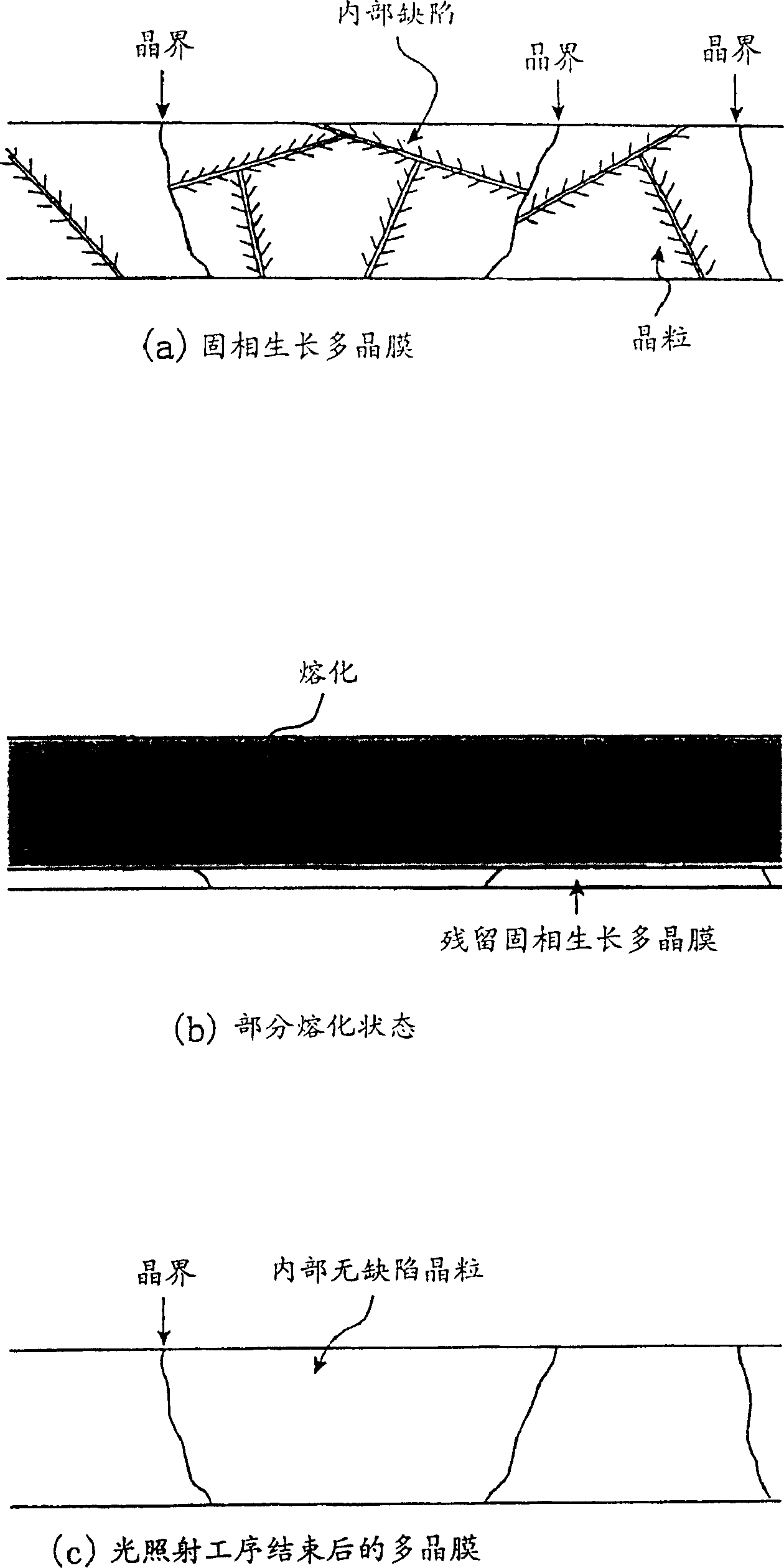
[0116] Figure 11 a to d are cross-sectional views showing the manufacturing process of a thin film semiconductor device forming a MOS-type electric field effect transistor. In the first embodiment, crystallized glass having a glass deformation point temperature of 750 degrees Celsius was used as the substrate 101 . However, even other substrates are not limited in their kind and size if they can withstand the highest temperature during the fabrication of thin film semiconductor devices. First, a silicon oxide film to be the base protective film 102 is deposited on the substrate 101 . When unnecessary impurities are included on the semiconductor film such as a ceramic substrate for the substrate, it is only necessary to deposit a first base protection film such as a tantalum oxide film and a silicon nitride film before depositing the silicon oxide film. In the first embodiment, a silicon oxide film of about 200 nm is deposited as the base protection film 102 on the substrate...

Embodiment 2

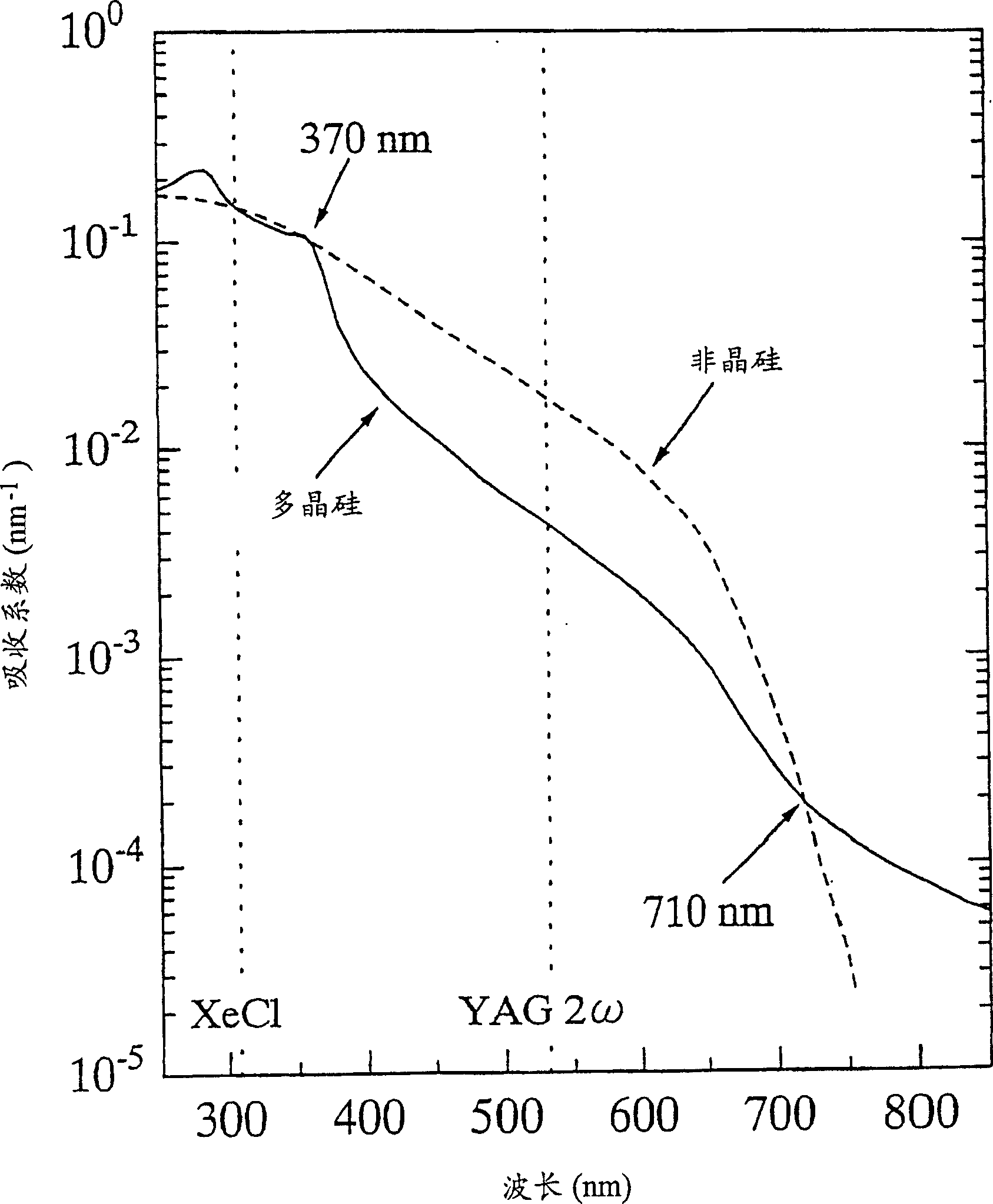
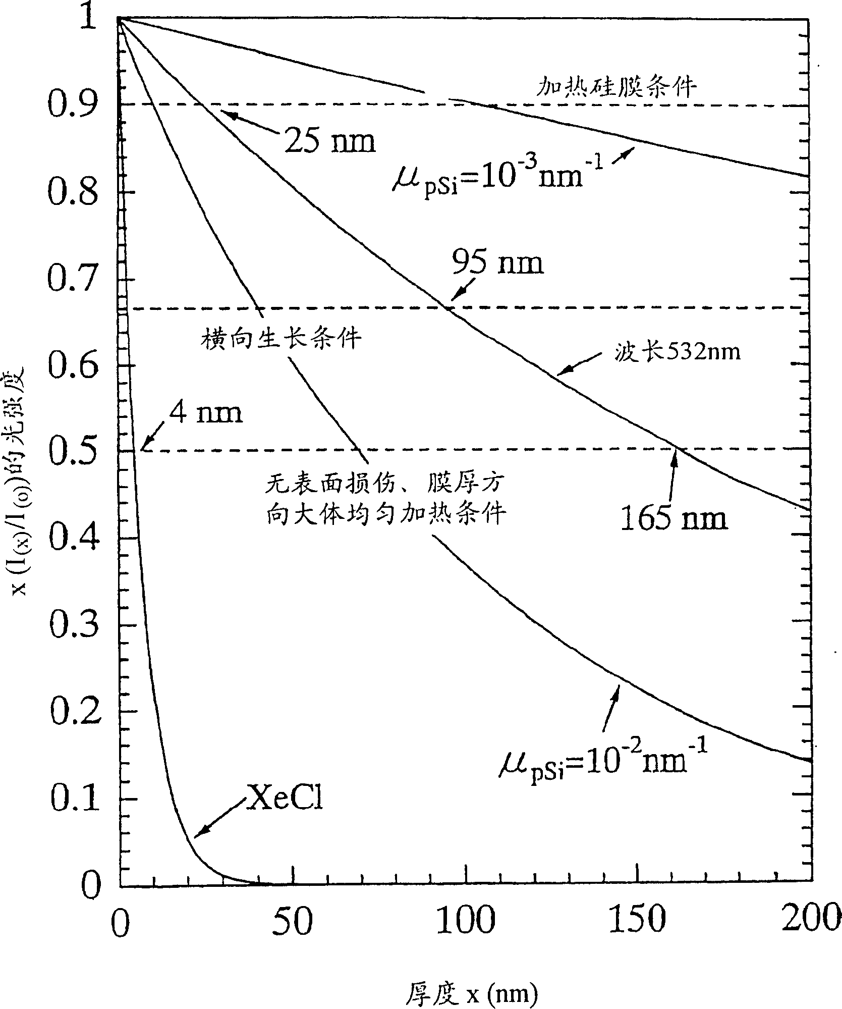
[0141] Except for irradiating the semiconductor film with the second harmonic wave of the pulsed Nd:YAG laser in the light irradiation process, the other manufacturing steps are exactly the same as in Example 1, so that a thin film semiconductor device can be produced. In Example 2, only the line-focused YAG2ω pulse laser with a width of 270 μm and a length of 10 mm is staggered in the width direction of each irradiation, and the laser irradiation energy density on the semiconductor film is different from that of Example 1. Four levels of 10%, 5%, 2.5%, and 1.67% are selected for the stagger ratio of the linear laser in the width direction of each irradiation. Accordingly, arbitrary points on the semiconductor film were irradiated with laser light about 10 times, 20 times, 40 times, and 60 times, respectively. The change in energy density of laser irradiation on the semiconductor film is 400mJ·cm -2 ~800mJ·cm -2 . The maximum change of the laser energy density gradient prop...


PUM

PropertyMeasurementUnit
Wavelengthaaaaaaaaaa

Abstract

The invention relates to manufacturing an excellent polycrystalline thin film semiconductor device under a comparatively lower temperature. After formation of an amorphous semiconductor film, it is crystallized in the solid phase. Thereafter, the crystallized amorphous semiconductor film is partly fused through irradiation of a pulse laser which exhibits absorption coefficient in the amorphous silicon which is higher than that in the polycrystalline silicon.

Description

technical field [0001] The present invention relates to a technique for forming an excellent polycrystalline semiconductor film with the best crystallization properties at a relatively low temperature below about 600 degrees Celsius; in particular, it relates to a manufacturing method for significantly improving the performance of semiconductor devices represented by polysilicon thin film transistors using this technique. Background technique [0002] When thin film semiconductor devices typified by polysilicon thin film transistors (p-Si TFTs) can be manufactured at low temperatures below 600 degrees Celsius using general-purpose glass substrates, the following manufacturing methods have been employed in the past. First, an amorphous silicon film to be a semiconductor film is deposited to a thickness of 50 nm on a substrate by a low-pressure chemical vapor deposition method (LPCVD method). Next, XeCl excimer laser light (wavelength: 308 nm) was irradiated on the amorphous f...

Claims


Application Information

Patent Timeline
IPC IPC(8): H01L21/20H01L21/324H01L21/336H01L29/768H01L29/786
Inventor 宫坂光敏时冈秀忠小川哲也
Owner SEIKO EPSON CORP
Why Eureka
Try Eureka