Vertical Diodes for Non-Volatile Memory Device

a technology of non-volatile memory and diodes, which is applied in the direction of diodes, semiconductor devices, magnetic field-controlled resistors, etc., can solve the problems of increasing power dissipation, non-scaling of sub-threshold slopes, and reducing device performan

Active Publication Date: 2012-12-06
INNOSTAR SEMICON SHANGHAI CO LTD
View PDF4 Cites 67 Cited by
  • Summary
  • Abstract
  • Description
  • Claims
  • Application Information

AI Technical Summary

Benefits of technology

[0010]In other implementations, the diode device can be configured in a memory cell to allow current to flow in a reversed bias of a switching device. This allows flexibility for applications in a wide range of switching materials, e.g. phase change chalcogenides, ReRAM metal oxides, and others. These switching materials may use a high voltage and a low current, or a high current and a low voltage, or other combinations for switching. Depending on the embodiment, these switching devices may be switched with the diode in reverse bias or forward bias. Further, the diode device also allows vertical stacking of multiple layers of switching devices and share an interconnect without disturb. Further details are described in the application “Architecture for 3D Memory.”

Problems solved by technology

However, as field effect transistors (FET) approach sizes less than 100 nm, problems such as the short channel effect degrade device performance.
Moreover, such sub 100 nm device sizes can lead to sub-threshold slope non-scaling and increase in power dissipation.
These devices often require new materials and device structures to couple with silicon-based devices to form a memory cell, which lack one or more key attributes.
For example, Fe-RAM and MRAM devices have fast switching characteristics and good programming endurance, but their fabrication is not CMOS compatible and size is usually large.
Additionally, switching a PCRAM device requires a large amount of power, and organic RAM or ORAM fabrication techniques are incompatible with large volume silicon-based fabrication and device reliability is usually poor.

Method used


Image

  • Vertical Diodes for Non-Volatile Memory Device
  • Vertical Diodes for Non-Volatile Memory Device
  • Vertical Diodes for Non-Volatile Memory Device

Examples


Embodiment Construction

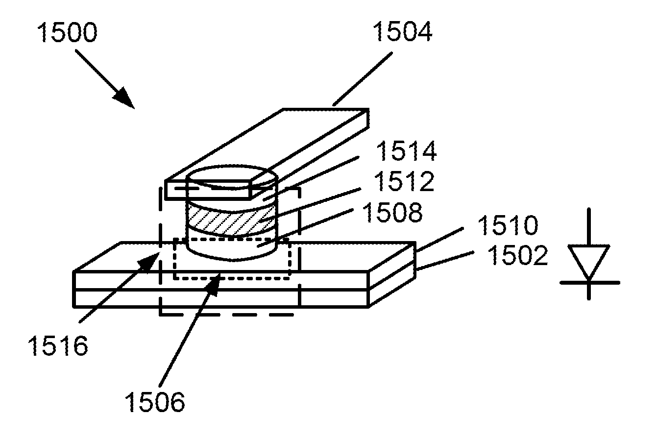
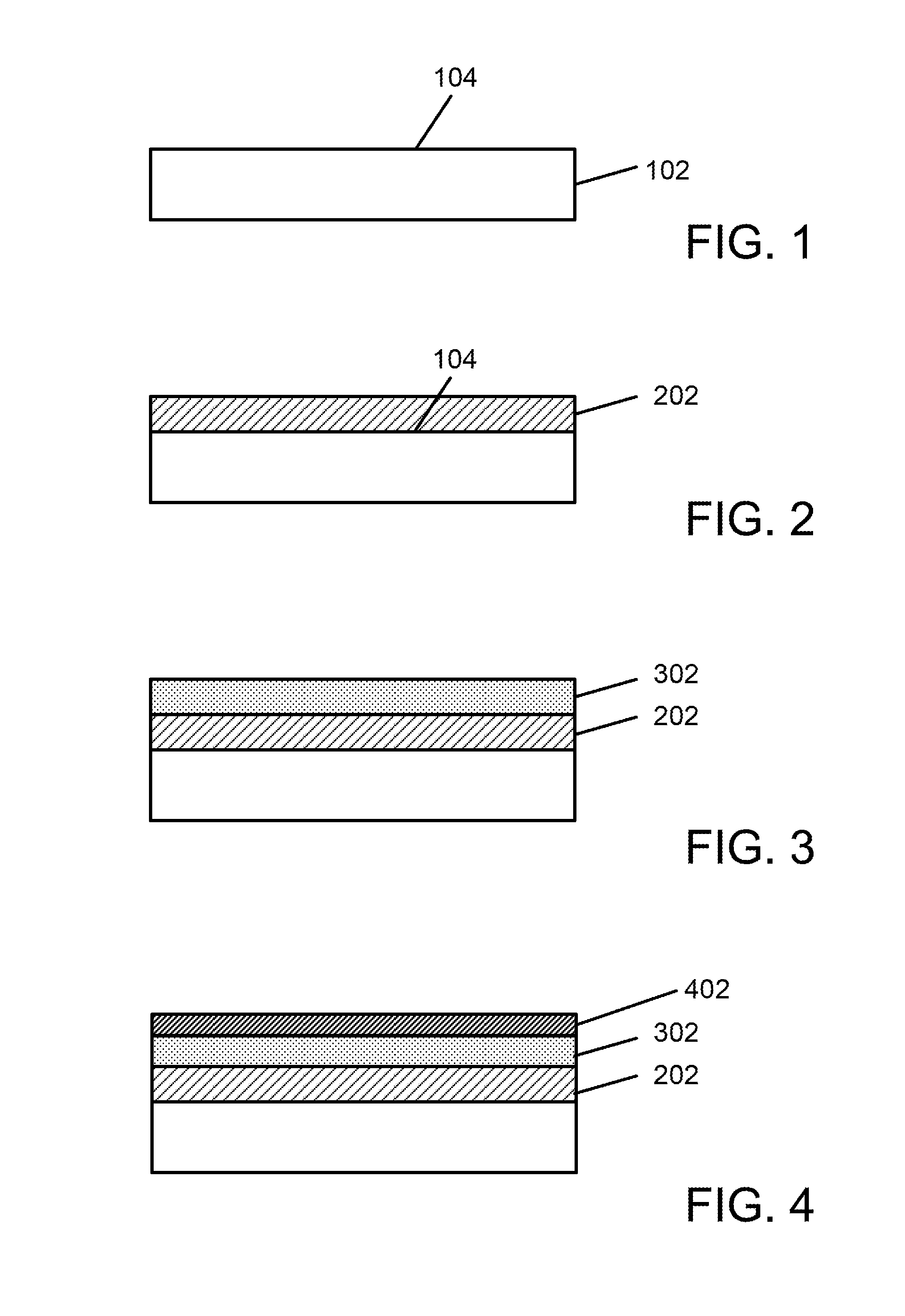
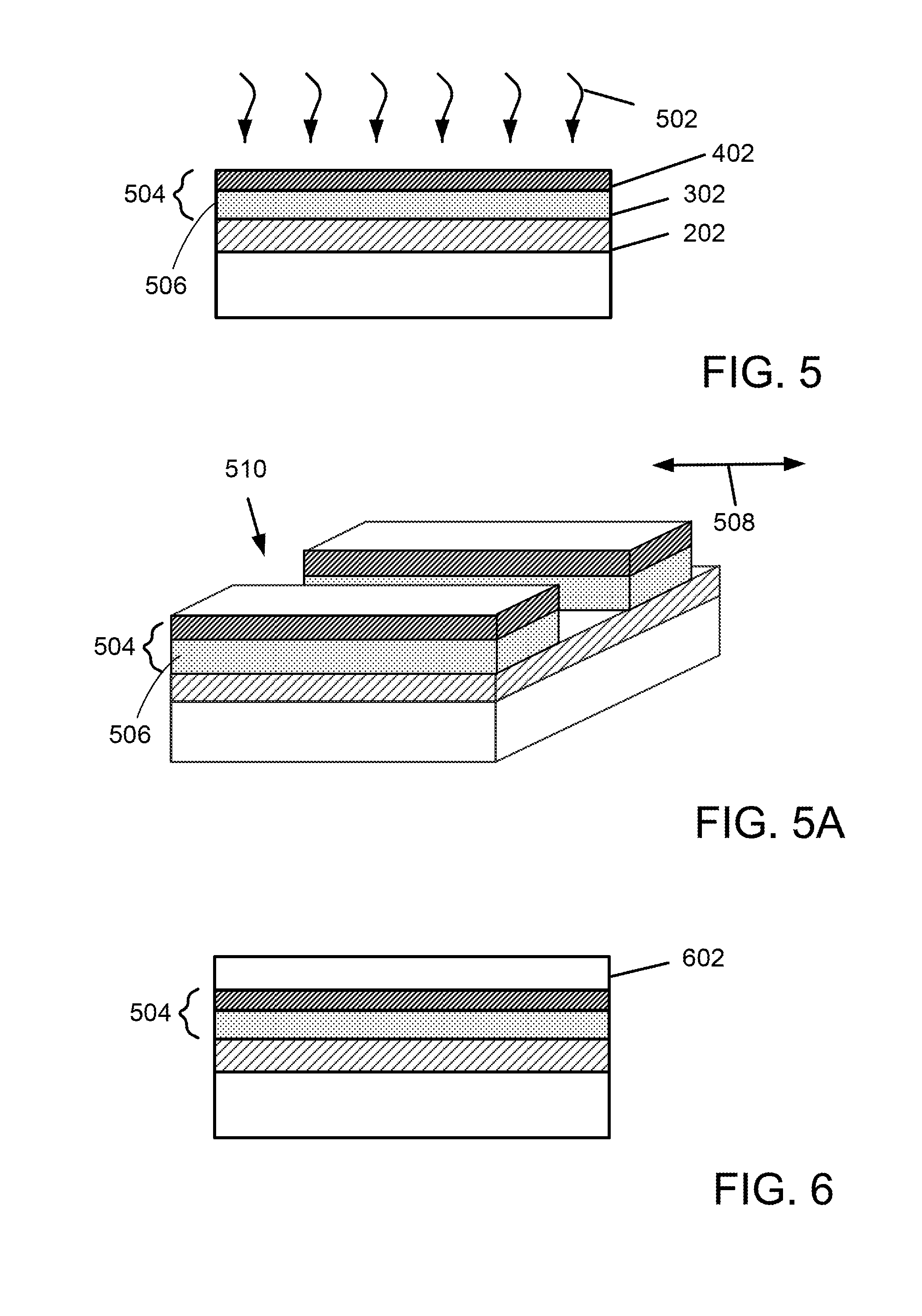
[0015]The present invention is generally related to steering elements. More particularly, embodiments according to the present invention provide a method and a device structure to form a rectifying element vertically integrated with a resistive switching device. The steering device can be fabricated at a process temperature less than about 450 Degrees Celsius. Embodiments according to the present invention can be applied to non-volatile memory devices, but it should be recognized that the present invention can have a much broader range of applicability.

[0016]High density and low cost storage devices are in ever increasing demand due to the growth in consumer devices common in the market place. Current non-volatile memory devices including Flash are probably at an end to further scaling due to fundamental limitations in the devices. It is predicted that current charge storage in a floating gate or a dielectric material in Flash devices may not be possible in device size less that abo...


PUM


Abstract

A steering device. The steering device includes an n-type impurity region comprising a zinc oxide material and a p-type impurity region comprising a silicon germanium material. A pn junction region formed from the zinc oxide material and the silicon germanium material. The steering device is a serially coupled to a resistive switching device to provide rectification for the resistive switching device to form a non-volatile memory device.

Description

CROSS REFERENCE TO RELATED APPLICATIONS[0001]The present invention is related-to and incorporates by reference, for all purposes, application Ser. No. 11 / 875,541 filed Oct. 19, 2007.BACKGROUND[0002]The present invention is generally related to steering elements for switching devices. More particularly, embodiments according to the present invention provide a method and a device structure to form a rectifying element that can be fabricated at low temperatures (<approximately 450C) and compatible with CMOS processing. Embodiments according to the present invention can be applied to non-volatile memory devices but it should be recognized that the present invention can have a much broader range of applicability.[0003]The success of semiconductor devices has been driven by an intensive transistor down-scaling process. However, as field effect transistors (FET) approach sizes less than 100 nm, problems such as the short channel effect degrade device performance. Moreover, such sub 100 ...

Claims


Application Information

Patent Timeline
Patent Type & Authority Applications(United States)
IPC IPC(8): H01L29/22H01L21/02
CPCH01L27/1021H01L29/16H01L29/24H01L43/08H01L29/8615H01L27/2409H01L29/267H10B63/20H10N50/10
Inventor HERNER, SCOTT BRAD
Owner INNOSTAR SEMICON SHANGHAI CO LTD
Why Eureka
Try Eureka