
DMOS transistor having an increased breakdown voltage and method for production

Active Publication Date: 2012-12-06
X FAB SEMICON FOUNDRIES +1
View PDF9 Cites 6 Cited by
  • Summary
  • Abstract
  • Description
  • Claims
  • Application Information

AI Technical Summary

Benefits of technology

[0016]Due to the additionally doped channel region a conductive path is established without applying a gate voltage. The implantation of the additional channel doping is preferably performed prior to forming the gate dielectric material, thereby avoiding any implantation induced damage in the gate dielectric material. For the subsequent implantation of the well region the gate electrode is used as an implantation mask, which has an appropriate structure so as to enable the incorporation of the well dopant species in the semiconductor material laterally adjacent to the gate electrode and also locally below the gate electrode structure, thereby enabling an increased lateral diffusion of the well dopant species without increasing the vertical diffusion. Hence, a desired increase in channel length may be obtained on the basis of the increased lateral diffusion caused by the well dopant species that is additionally provided locally below the gate electrode structure. The increased channel length in turn may compensate for the additionally doped channel region in terms of punch through voltage, while not unduly increasing a depth of the well region.
[0037]In a further embodiment an additional channel dopant species is incorporated prior to forming the gate electrode structure. In this manner a depletion mode channel region may be provided without unduly affecting the sensitive gate dielectric material.

Problems solved by technology

However, implanting the additional dopants through the gate electrode or even through the gate dielectric material may result in significant damage of the gate dielectric material, thereby deteriorating the overall transistor performance.
In particular, a pronounced vertical diffusion into the well region 5 will occur, thereby negatively affecting the overall transistor behaviour.
When switching off the transistor, however, an early breakdown may occur, since the effective well doping is reduced due to the additional channel doping even if strongly negatively biased.
For example, an increased channel length is obtained by increasing the diffusion activity during the well diffusion, thereby, however, not only increasing the lateral diffusion and thus the channel length, but also increasing the vertical extension to of the well region, which may result in a non-desired change of the transistor's characteristics.

Method used


Image

  • DMOS transistor having an increased breakdown voltage and method for production
  • DMOS transistor having an increased breakdown voltage and method for production
  • DMOS transistor having an increased breakdown voltage and method for production

Examples


Embodiment Construction

[0039]The embodiments support the understanding of the invention(s) as claimed. They are not “the invention”, but examples (embodiments) thereof.

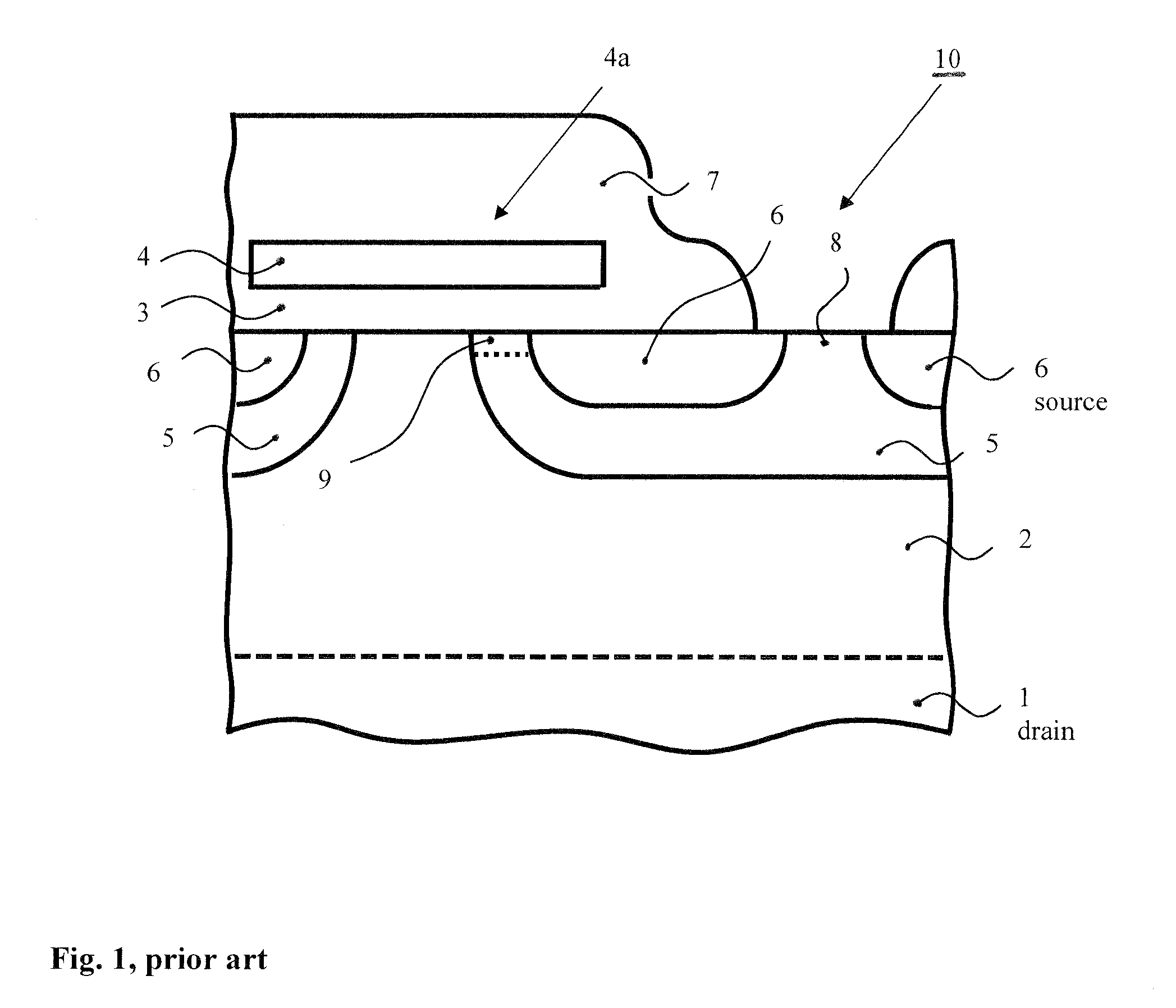
[0040]FIG. 1 schematically illustrates a cross-sectional view of a vertical DMOS transistor as an enhancement mode type according to conventional transistor architecture,

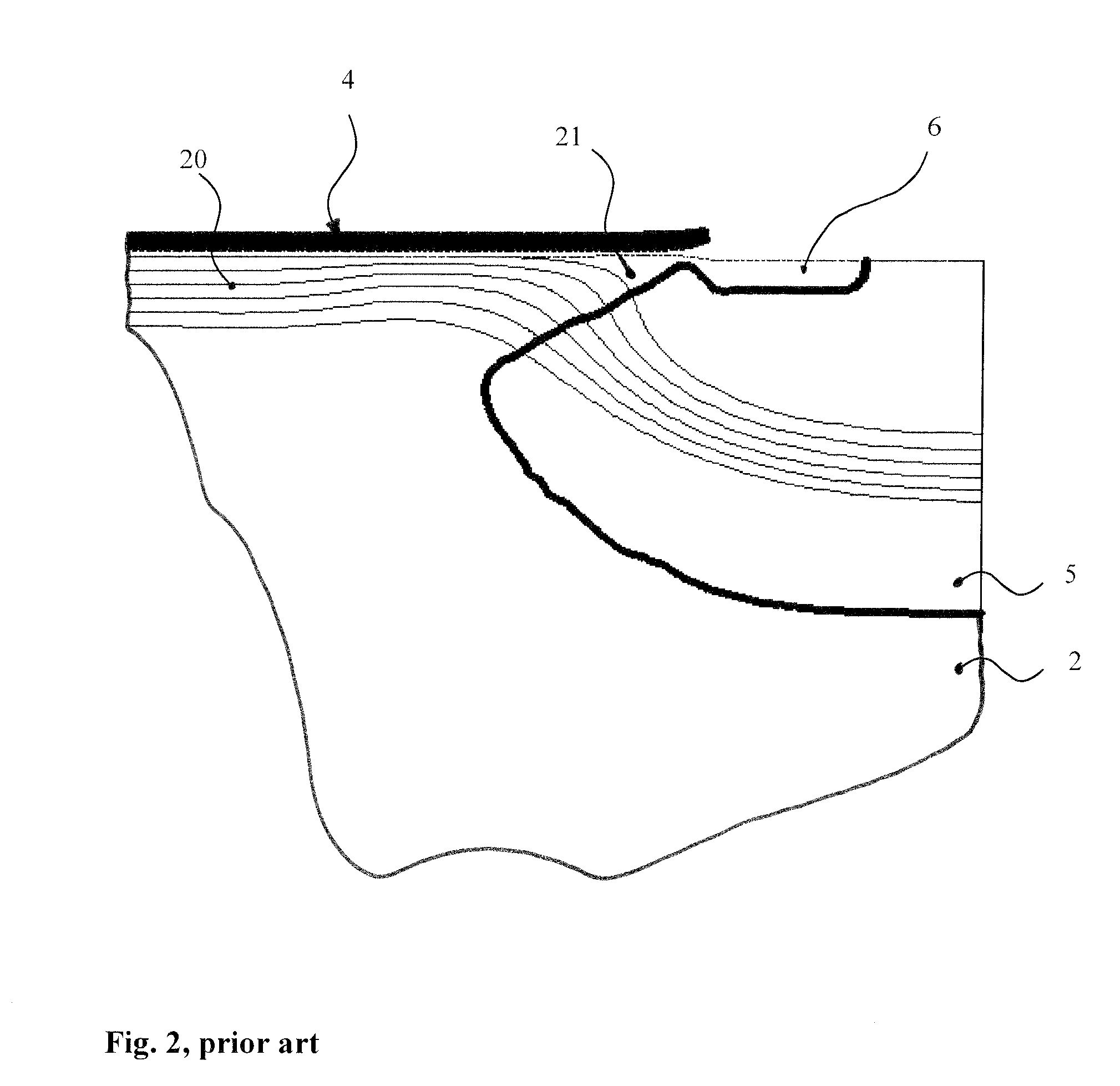
[0041]FIG. 2 schematically illustrates a (voltage) potential in off state in a known transistor having an additionally doped channel region to obtain a depletion type DMOS transistor, thereby reducing punch through voltage,

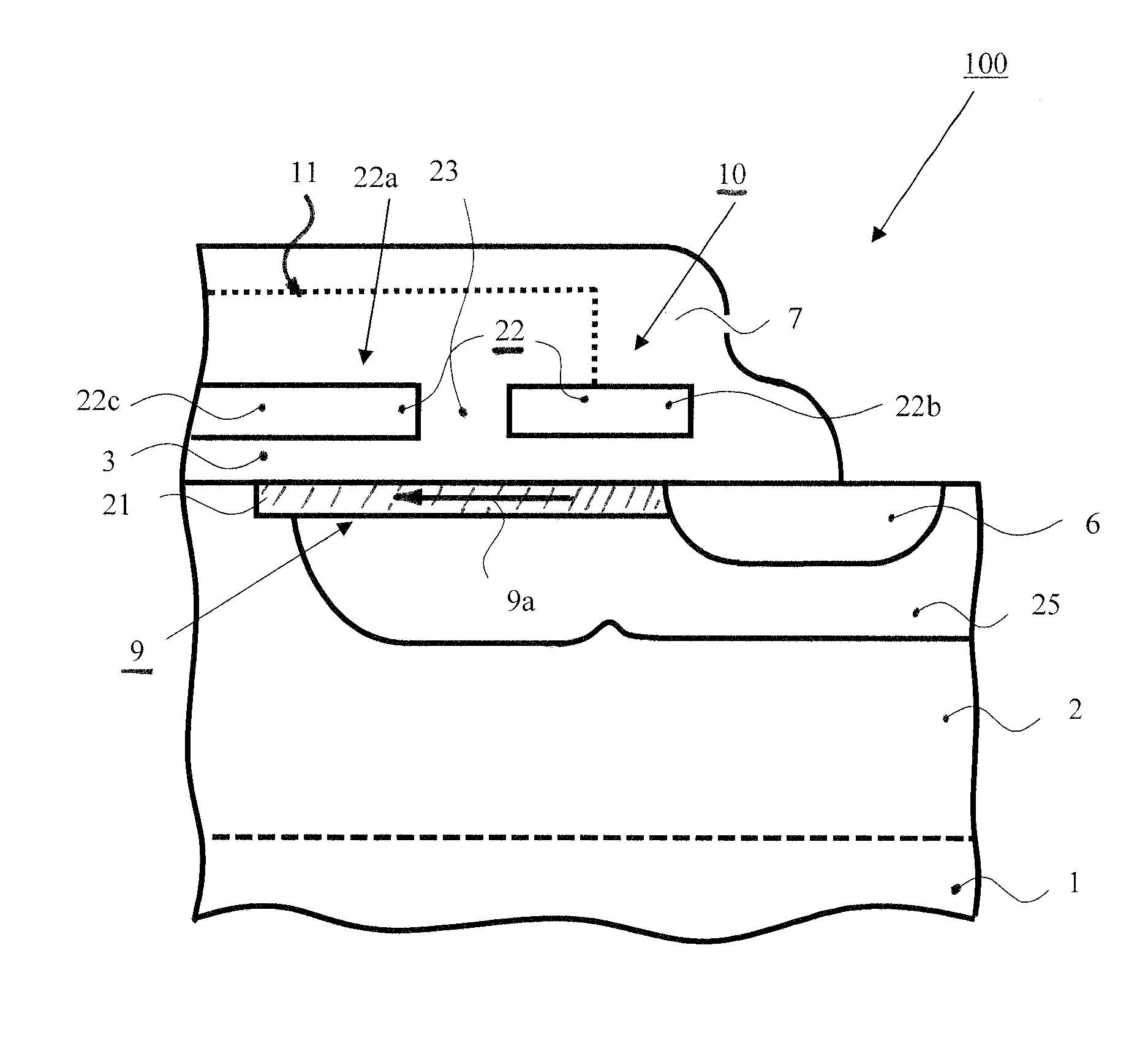
[0042]FIG. 3 schematically illustrates a cross-sectional view of a new DMOS transistor of the depletion type including an increased channel length, while the well region has a desired vertical extension,

[0043]FIG. 4 schematically illustrates the (off state voltage) potential in the transistor having an additional channel region and a gapped gate electrode, wherein early punch through may be avoided,

[0044]FIG. 5 schematically illustrates a perspective view...


PUM


Abstract

A depletion type DMOS transistor comprises a gap in electrode material allowing incorporation of a well dopant species into the underlying semiconductor material. During subsequent dopant diffusion a continuous well region is obtained having an extended lateral extension without having an increased depth. The source dopant species is implanted after masking the gap. Additional channel implantation is performed prior to forming the gate dielectric material.

Description

TECHNICAL FIELD[0001]The invention as claimed relates to a DMOS (double-diffused metal oxide semiconductor) transistor as depletion type, or configured to be operated in the depletion mode, in which a conductive channel is formed without applying a voltage to the gate electrode structure.BACKGROUND[0002]Generally field effect transistors (FET), specifically MOS transistors are semiconductor devices that comprise a source terminal and a drain terminal and an intermediate channel region, in which a conductive channel forms upon applying an appropriate control voltage to a gate electrode structure. The gate electrode structure in turn includes a gate electrode and a gate dielectric layer that separates the gate electrode from the channel region. By applying a voltage across the gate electrode and the semiconductor body that is connected to the channel region, exceeding the threshold voltage of the transistors charge carriers increasingly accumulate at the interface formed by the gate d...

Claims


Application Information

Patent Timeline
IPC IPC(8): H01L29/78H01L21/336
CPCH01L29/0623H01L29/42376H01L29/7828H01L29/66666H01L29/4238
Inventor LERNER, RALFHOWER, PHILKITTLER, GABRIELSCHOTTMANN, KLAUS
Owner X FAB SEMICON FOUNDRIES
Features
  • Generate Ideas
  • Intellectual Property
  • Life Sciences
  • Materials
  • Tech Scout
  • Unparalleled Data Quality
  • Higher Quality Content
  • 60% Fewer Hallucinations
Learn More