Semiconductor device with spacer layer between carrier traveling layer and carrier supplying layer

a technology of spacer layer and carrier, which is applied in the direction of semiconductor devices, basic electric elements, electrical devices, etc., can solve the problems of degrading the mobility of the carrier, and achieve the effect of improving the surface flatness of the doped layer and the sheet resistance of the 2deg

Active Publication Date: 2012-12-13
SUMITOMO ELECTRIC IND LTD
View PDF6 Cites 20 Cited by
  • Summary
  • Abstract
  • Description
  • Claims
  • Application Information

AI Technical Summary

Benefits of technology

[0008]One aspect of the present invention relates to a semiconductor device that includes a substrate, a channel layer, a spacer layer, and a doped layer, where they are stacked on the substrate in this order to form a 2DEG in the channel layer at the interface to the spacer layer. The channel layer may be made of a nitride semiconductor material, typically, GaN. A feature of the embodiment is that the spacer layer has a thickness thicker than, or equal to, 0.5 nm but thinner than, or equal to, 1.25 nm. Further preferably, the thickness of the spacer layer is less than, or equal to, 0.8 nm to improve the sheet resistance of the 2DEG and the surface flatness of the doped layer consistently.

Problems solved by technology

However, the lattice mismatching of AlGaN doped layer becomes large as the Al composition increases, which degrades the mobility of the carrier in 2DEG and the sheet resistance thereof oppositely increases.

Method used


Image

  • Semiconductor device with spacer layer between carrier traveling layer and carrier supplying layer
  • Semiconductor device with spacer layer between carrier traveling layer and carrier supplying layer
  • Semiconductor device with spacer layer between carrier traveling layer and carrier supplying layer

Examples


first embodiment

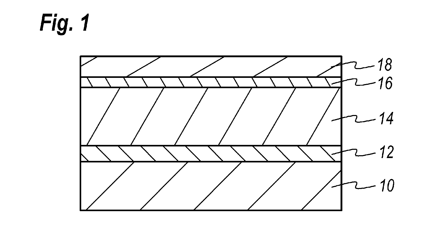
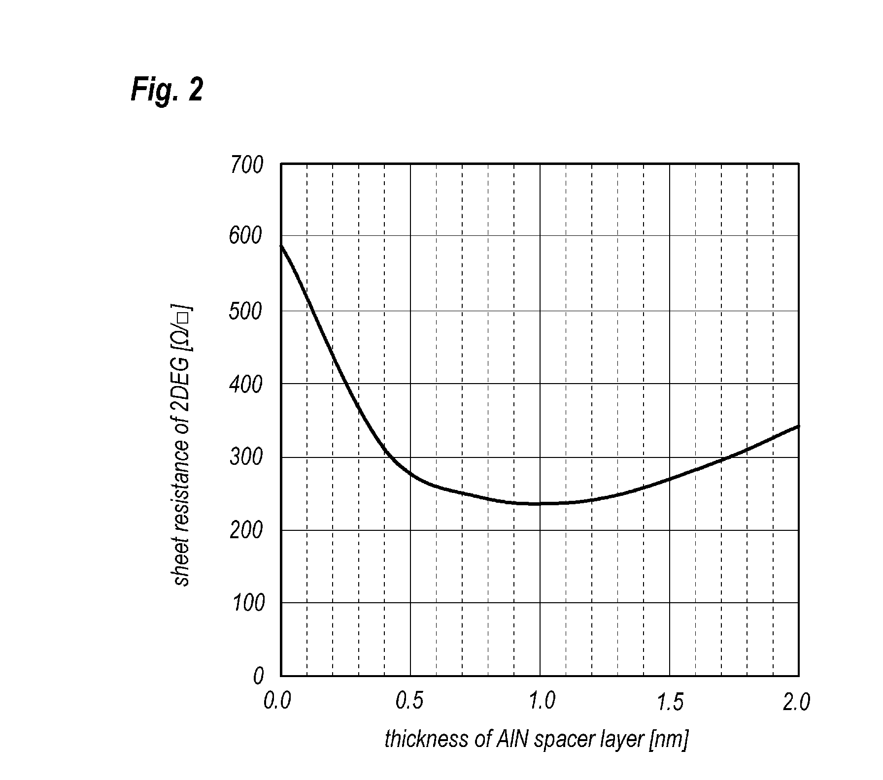
[0022]Experiments performed to evaluate a thickness of the spacer layer will be firstly described. FIG. 1 is a cross section of epitaxially grown layers for investigating a relation of the sheet resistance of the 2DEG against the surface morphology of the doped layer, which is made of InAlN to supply carriers into the 2DEG. The epitaxial layers may be grown by, for instance, the metal organic chemical vapor deposition (MOCVD).

[0023]Referring to FIG. 1 and table 1 below described, a substrate 10 made of SiC is set within the growth chamber of the MOCVD apparatus; then, a series of layers from AlN buffer layer 12 to AlN spacer layer 16 are sequentially grown on the SiC substrate 10 under conditions of the source materials by hydrogen (H) without any annotations as a carrier gas, the growth temperature, and the thickness of respective layer shown in table 1. In table 1, TMA, TMG, and TMI each means tri-methyl-aluminum, tri-methyl-gallium, and tri-methyl-indium.

TABLE 1growth conditions ...

second embodiment

[0045]Next, conditions for growing InAlN doped layer will be investigated. As described above, the thickness of AlN spacer layer strongly depends of the surface morphology of InAlN doped layer; however, other factors also affect the surface flatness and morphology of InAlN doped layer. One factor is a partial pressure of ammonia gas against the total pressure of source gasses when InAlN doped layer is grown.

[0046]Experiments to investigate the partial pressure of ammonia first prepared specimens each grown under conditions shown in table 3 below:

TABLE 3growth conditions of respective layerslayerSourceTtSiC substrate 10AlN layer 12TMA, NH31000° C.300 nmAlGaN layer 13TMA, TMG, NH31000° C.150 nmAl composition 50%GaN channel layer 14TMG, NH31000° C.500 nmNH3 partialpressure 0.5InAlN doped layer 18TMI, TMA, NH3 750° C. 10 nmIn composition 17%NH3 partialpressure 0.1-0.5

[0047]The AlN layer 12 and AlGaN layer 13 correspond to the buffer layer 12 in the aforementioned embodiment. The process...


PUM


Abstract

A nitride semiconductor device is disclosed. The device includes a stack of semiconductor layers including the channel layer, the spacer layer, and the doped layer. The spacer layer is made of AlN while the doped layer is InAlN. A feature of the embodiment is that the spacer layer has a thickness of 0.5 to 1.25 nm.

Description

BACKGROUND OF THE INVENTION[0001]1. Field of the Invention[0002]The present invention relates to a semiconductor device, in particular, one embodiment of the semiconductor device is, what is called, the high-electron mobility transistor (HEMT) formed by nitride semiconductor materials.[0003]2. Related Prior Arts[0004]Nitride semiconductor materials have been applicable to a power device showing a high output in higher frequencies. One prior art has disclosed a HEMT that includes a buffer layer, GaN carrier traveling layer, which is often called as a channel layer, AlGaN carrier supplying layer, which is sometimes called as doped layer, each layers being sequentially grown on a substrate, and utilizes a two dimensional electron gas (2DEG) formed in the channel layer at an interface against the doped layer.[0005]In order to improve the high frequency performance of HEMT device further, the trans-conductance of the device is necessary to be enhanced. Specifically, the sheet resistance ...

Claims


Application Information

Patent Timeline
Patent Type & Authority Applications(United States)
IPC IPC(8): H01L29/778H01L21/20
CPCH01L21/02378H01L21/02458H01L21/02505H01L21/0254H01L29/7783H01L21/0262H01L29/2003H01L29/66462H01L21/02573
Inventor MAKABE, ISAO
Owner SUMITOMO ELECTRIC IND LTD
Why Eureka
Try Eureka