Memory array with local bitlines and local-to-global bitline pass gates and gain stages

a memory array and global bitline technology, applied in the field of memory, can solve the problems of reducing the p/e cycle that floating gate transistors can endure, the fundamental limit to the extent to which floating gate transistors can be scaled without suffering data retention problems, etc., and achieve the effect of high ra

Active Publication Date: 2012-12-13
UNITY SEMICON
View PDF8 Cites 65 Cited by
  • Summary
  • Abstract
  • Description
  • Claims
  • Application Information

AI Technical Summary

Benefits of technology

[0008]During times when a selected memory element is being programmed or erased, the LBL associated with the selected memory element is electrically coupled with an associated GBL via one of the switching devices. During times when a selected memory element is being read, the switching device associated with the LBL is switched opened so that the LBL is electrically isolated from its associated GBL, and a read voltage is then applied across the selected memory element. The applied read voltage causes current to flow through the selected memory element and charge the capacitance of the LBL to a local bit line voltage. The local bit line voltage depends on the memory state of the selected memory element and is amplified by the gain stage and conducted along the GBL that is associated with the LBL. The amplified current, or other related signal on the GBL, is then sensed by a sense amplifier or measured by some other measuring circuit, to determine the stored memory state of the selected memory element. In addition to performing an amplifying function, the gain stage serves to isolate the capacitances of the LBL from the much larger capacitance of the associated GBL. Together, the amplification and isolation functions of the amplifiers allow data to be read from the memory array at a high rate.
[0009]According to one aspect of the invention, the plurality of switching devices, plurality of amplifiers, plurality of GBLs, and other supporting logic used to exercise and control the operation of the memory array are formed in a semiconductor substrate or in a semiconductor epitaxial layer, in accordance with a front-en

Problems solved by technology

Only so many of these program and erase (P/E) cycles can be performed before the thin tunnel dielectric layer wears out and the floating gate transistor is no longer able to reliably store charge.
The number of P/E cycles that floating gate transistors can endure decreases with scaling, and in recent years there has been shown to be a fundamental limit to the extent to which floating gate transistors can

Method used


Image

  • Memory array with local bitlines and local-to-global bitline pass gates and gain stages
  • Memory array with local bitlines and local-to-global bitline pass gates and gain stages
  • Memory array with local bitlines and local-to-global bitline pass gates and gain stages

Examples


Embodiment Construction

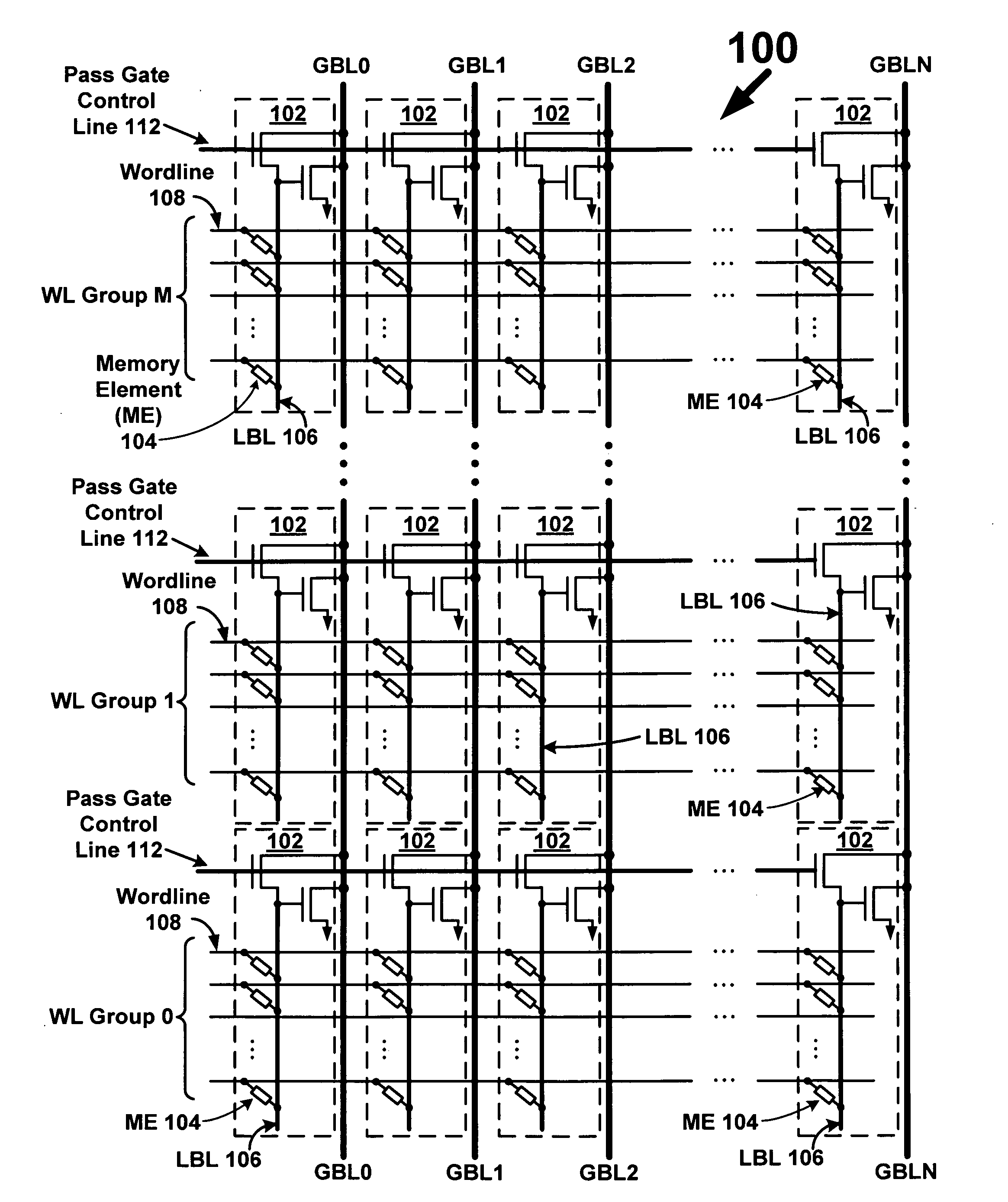
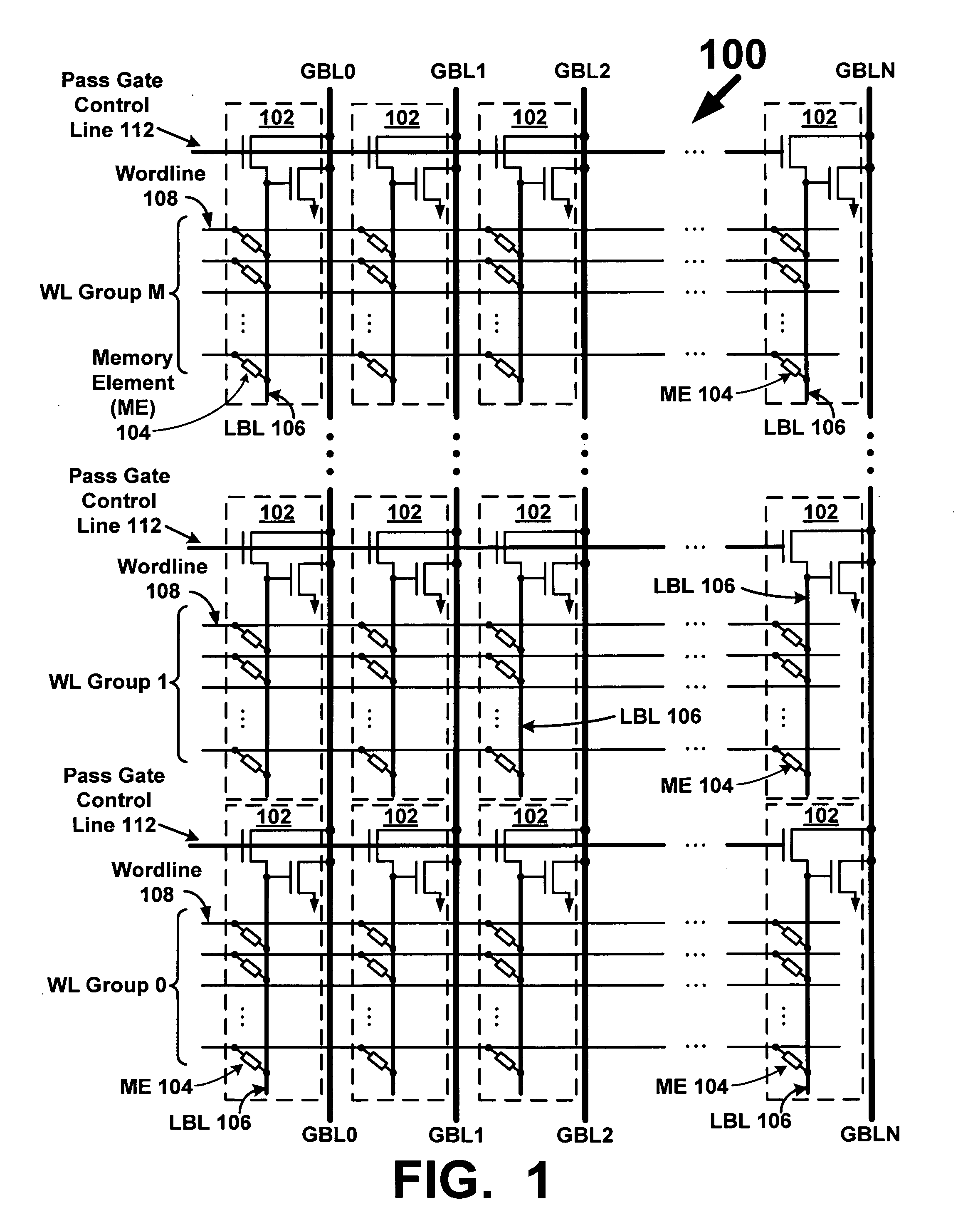
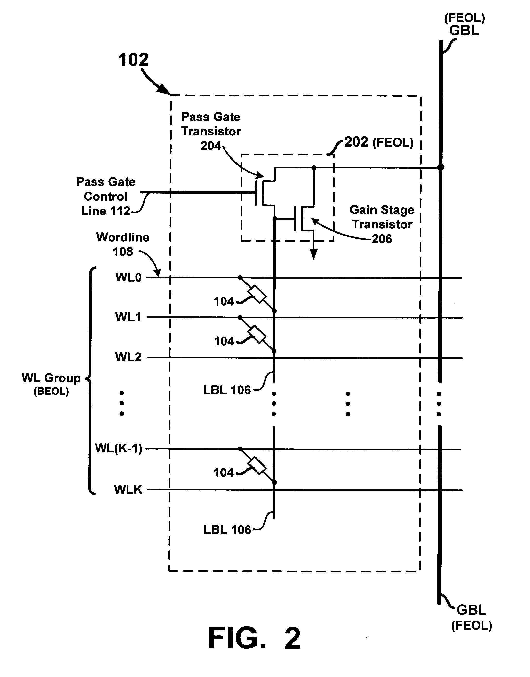
[0031]Referring to FIG. 1 there is shown a memory array 100, according to an embodiment of the present invention. The memory array 100 comprises a plurality of memory array portions 102, each associated with one of (M+1) wordline (WL) groups and one of N+1 global bitlines (GBLs) GBL0, GBL1, . . . , GBLN, where M and N are integers greater than or equal to zero. As can be observed in the more detailed drawing of the memory array portion 102 in FIG. 2, each memory array portion 102 includes a local bitline (LBL) 106, a pass gate transistor 204, and a gain stage transistor 206. K+1 memory elements 104 are coupled between each LBL 106 and K+1 WLs 108 of an associated WL group, where K is an integer greater than or equal to zero. The number of memory elements 104 per LBL 106 is set during design and determined by a number of factors, including but not limited to: overall memory array size, required operation parameters, program and / or erase operation parameters, type of memory elements 1...


PUM


Abstract

A memory array includes wordlines, local bitlines, two-terminal memory elements, global bitlines, and local-to-global bitline pass gates and gain stages. The memory elements are formed between the wordlines and local bitlines. Each local bitline is selectively coupled to an associated global bitline, by way of an associated local-to-global bitline pass gate. During a read operation when a memory element of a local bitline is selected to be read, a local-to-global gain stage is configured to amplify a signal on or passing through the local bitline to an amplified signal on or along an associated global bitline. The amplified signal, which in one embodiment is dependent on the resistive state of the selected memory element, is used to rapidly determine the memory state stored by the selected memory element.

Description

FIELD OF THE INVENTION[0001]The present invention relates generally to memory. More particularly, the present invention relates to non-volatile memory arrays and to methods and apparatus for performing data operations on memory elements of non-volatile memory arrays.BACKGROUND OF THE INVENTION[0002]Flash memory is a type of non-volatile memory (NVM) used extensively as secondary storage and long-term persistent storage of electronic data. It is also widely used to store firmware of computers (e.g., the basic input-output operating system (BIOS) of personal computers) and other electronic devices. In addition to being non-volatile, Flash memory is electrically re-writable and requires no moving parts. These attributes have made Flash memory popular for use in portable and battery-powered electronic devices, such as tablet and notebook computers, cell phones, smart phones, personal digital assistants, digital audio players and digital cameras.[0003]Increased processing capability and ...

Claims


Application Information

Patent Timeline
IPC IPC(8): G11C5/06G11C5/08B82Y10/00
CPCG11C5/06G11C7/00G11C16/00G11C7/18G11C2213/71G11C13/0007G11C13/0011G11C13/0026G11C13/0004
Inventor SIAU, CHANG HUABATEMAN, BRUCE
Owner UNITY SEMICON
Why Eureka
Try Eureka