Metal gate and fabrication method thereof

a metal gate and fabrication method technology, applied in the direction of basic electric elements, electrical equipment, semiconductor devices, etc., can solve the problems of inferior performance, reduced gate capacitance, and conventional polysilicon gates, and achieve the effect of improving the electrical quality of metal gates and low work functions

a metal gate and fabrication method technology, applied in the direction of basic electric elements, electrical equipment, semiconductor devices, etc., can solve the problems of inferior performance, reduced gate capacitance, and conventional polysilicon gates, and achieve the effect of improving the electrical quality of metal gates and low work functions

US20120319179A1Inactive Publication Date: 2012-12-20UNITED MICROELECTRONICS CORP

Image

  • Metal gate and fabrication method thereof
  • Metal gate and fabrication method thereof
  • Metal gate and fabrication method thereof

Examples


Embodiment Construction

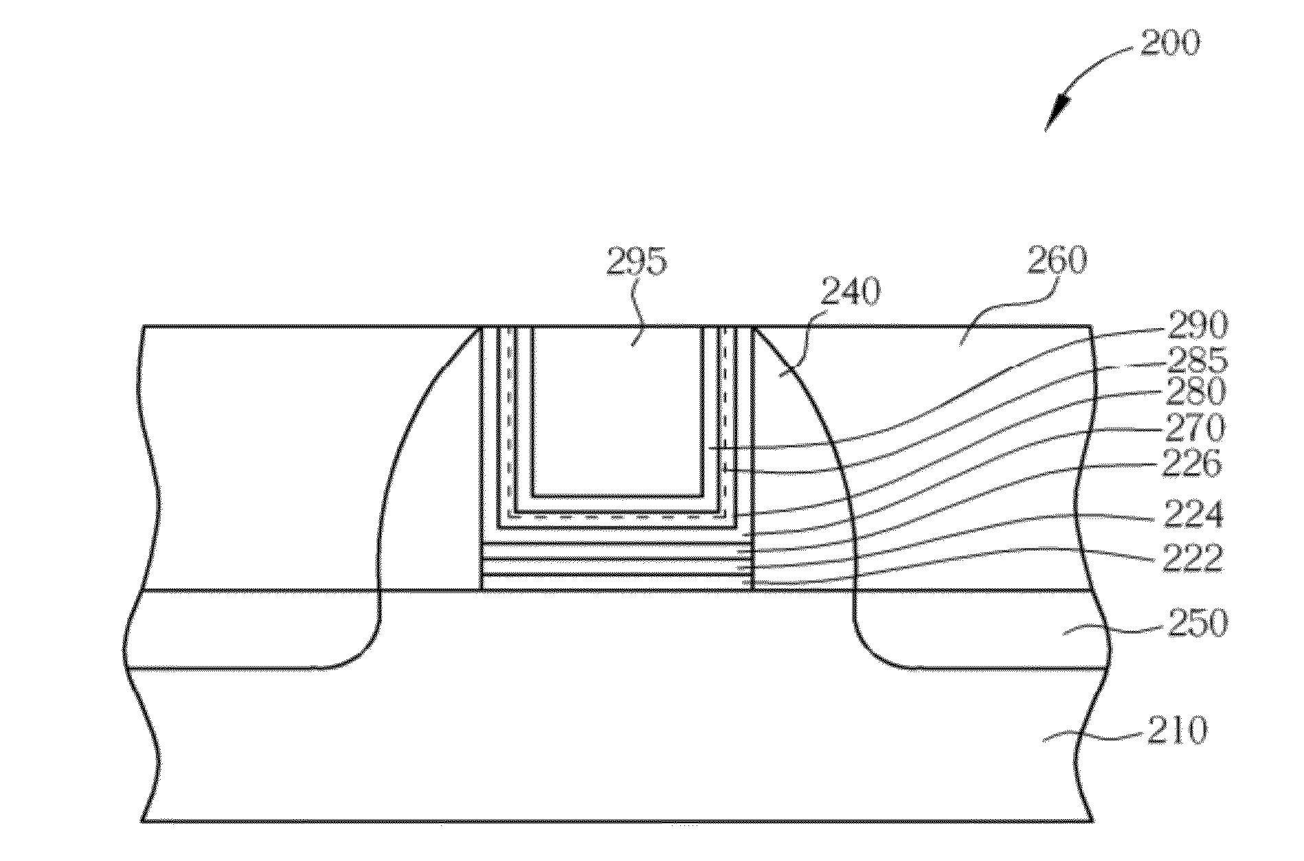
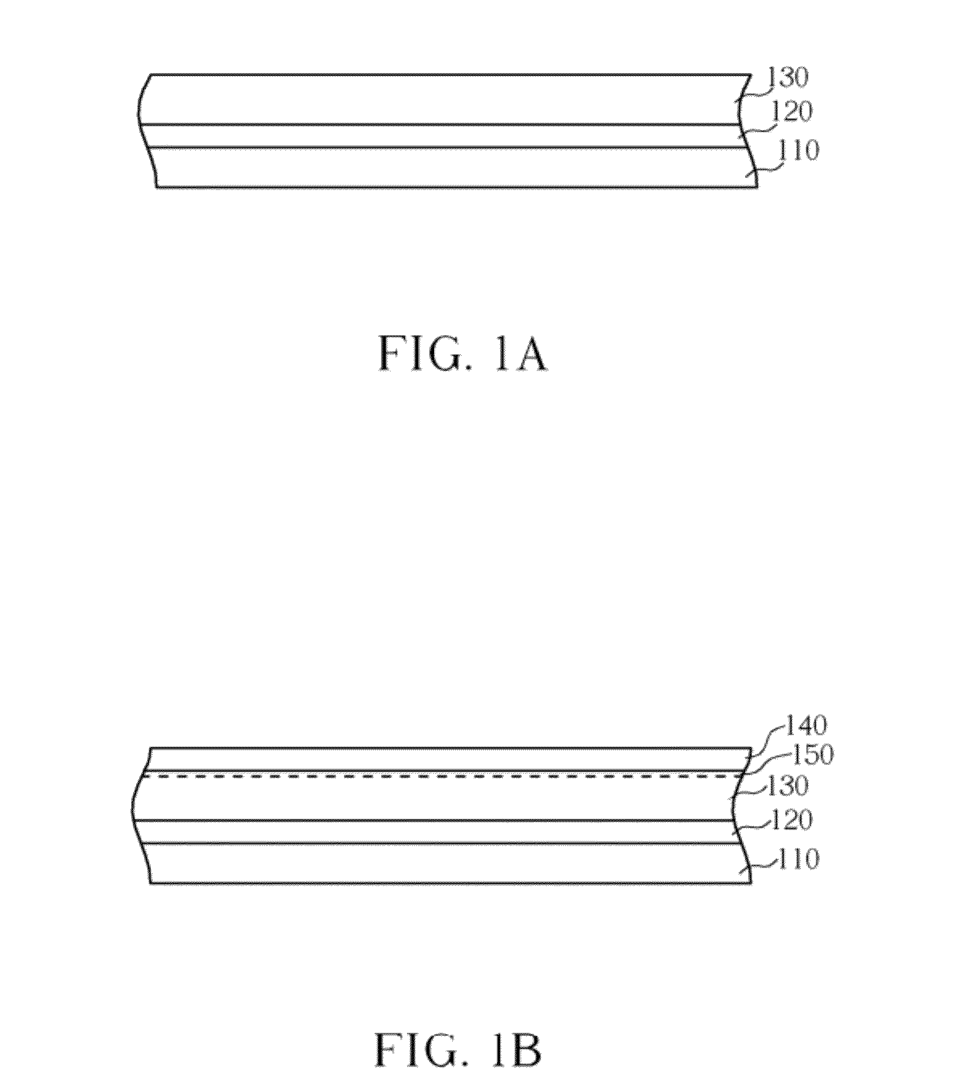
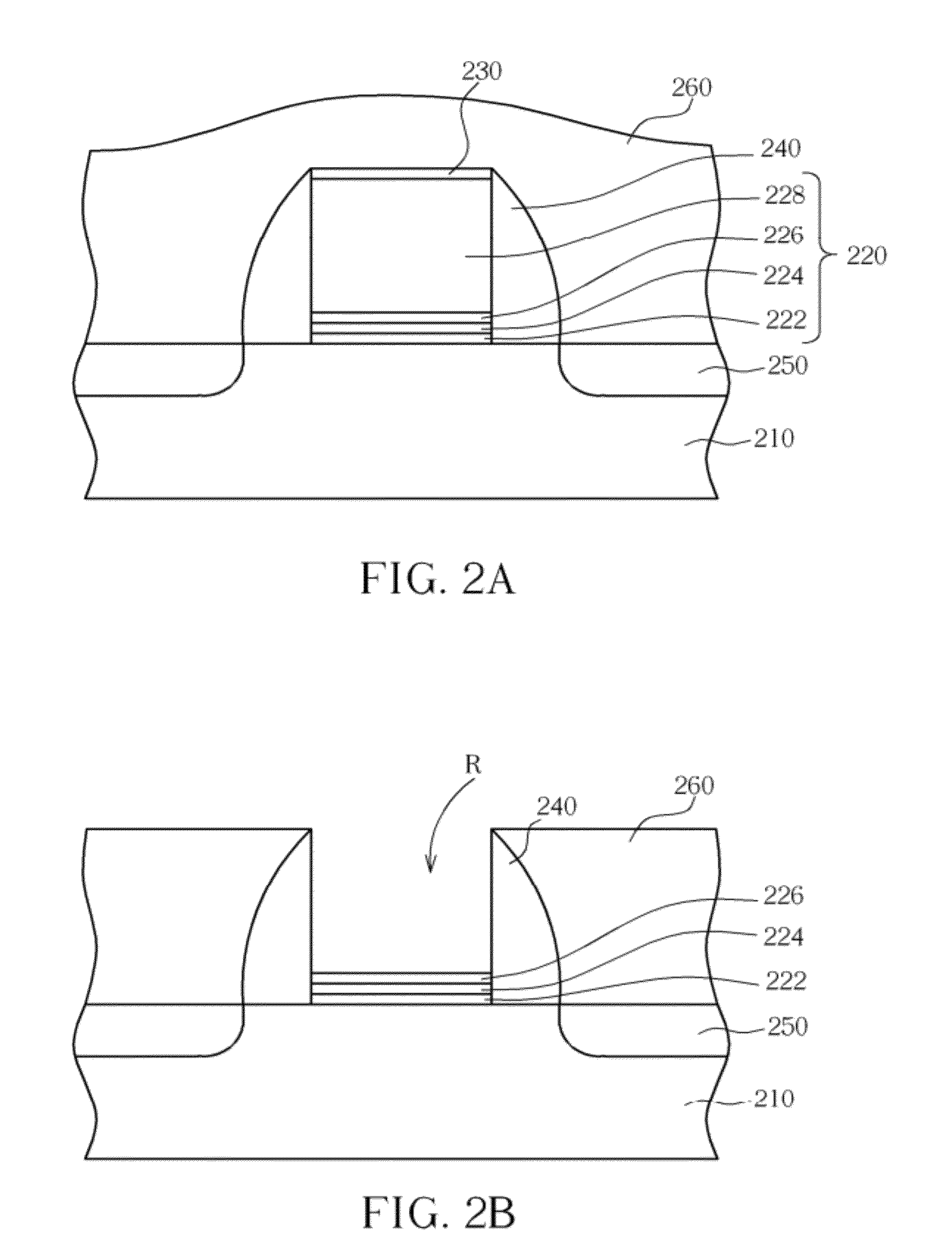
[0016]FIG. 1A-1B schematically depicts a cross-sectional view of a metal gate process according to the first embodiment of the present invention. Please refer to FIG. 1A-1B. As shown in FIG. 1A, a substrate 110 is provided and a gate dielectric layer 120 is formed on the substrate 110, wherein the substrate 110 may be a semiconductor substrate such as a silicon substrate, a silicon-containing substrate or a silicon-on-insulator (SOI) substrate, and the gate dielectric layer 120 may be a stack structure with a single layer or multilayered. Otherwise, a buffer interface layer (not shown) may be formed before the gate dielectric layer 120 is formed, to buffer and connect the substrate 110 and the gate dielectric layer 120, wherein the material of the buffer interface layer may be silicon dioxide. In this embodiment, the gate dielectric layer 120 may be, but is not limited to, a gate dielectric layer having a high-k dielectric constant, and the gate dielectric layer having a high-k diel...


PUM

PropertyMeasurementUnit
work functionaaaaaaaaaa
thicknessaaaaaaaaaa
work functionaaaaaaaaaa

Abstract

A metal gate includes a substrate, a gate dielectric layer, a work function metal layer, an aluminum nitride layer and a stop layer. The gate dielectric layer is located on the substrate. The work function metal layer is located on the gate dielectric layer. The aluminum nitride layer is located on the work function metal layer. The stop layer is located on the aluminum nitride layer.

Description

BACKGROUND OF THE INVENTION[0001]1. Field of the Invention[0002]The present invention relates generally to a metal gate and fabrication method thereof, and more specifically, to a stop layer in-situ forming on a work function metal layer, forming a metal gate structure, and a fabrication method thereof.[0003]2. Description of the Prior Art[0004]Poly-silicon is conventionally used as a gate electrode in semiconductor devices, such as the metal-oxide-semiconductor (MOS). However, with a trend toward scaling down the size of semiconductor devices, the conventional poly-silicon gate has faced problems such as inferior performance due to boron penetration and an unavoidable depletion effect which increases the equivalent thickness of the gate dielectric layer, reduces gate capacitance, and worsens a driving force of the devices. Therefore, work function metals have been used to replace the conventional poly-silicon gate, to act as the control electrodes suitable for use as the high-K gat...

Claims


Application Information

Patent Timeline
20 Dec 2012
Publication
US20120319179A1
IPC
H01L21/28; H01L29/78
CPC
H01L21/28088; H01L29/4966; H01L29/66545; H01L29/518; H01L29/517
Inventors
HUANG, HSIN-FU; LEE, ZHI-CHENG