Semiconductor devices having vertical device and non-vertical device and methods of forming the same

Active Publication Date: 2012-12-20
SAMSUNG ELECTRONICS CO LTD +1
View PDF2 Cites 107 Cited by
  • Summary
  • Abstract
  • Description
  • Claims
  • Application Information

AI Technical Summary

Benefits of technology

[0007]Other embodiments of the inventive concepts provide a static random access memory

Problems solved by technology

With the growing tendency for MOSFETs to have channel lengths of about 100 nm or less, the fabrication of semiconductor devices having both a high driving current and a low off-leakage current has become increasingly difficult due to a phenomenon kn

Method used


Image

  • Semiconductor devices having vertical device and non-vertical device and methods of forming the same
  • Semiconductor devices having vertical device and non-vertical device and methods of forming the same
  • Semiconductor devices having vertical device and non-vertical device and methods of forming the same

Examples


embodiment 1

[0182]In an ultrathin body (UTB) SOI device or in a nanowire device, which are expected to be applied in the future to sub-20 nm devices, since the dopant of a channel region has little effect on the threshold voltage VT of the resulting device, such devices still do not solve the problem of heightened leakage current. Further, the approach of controlling the threshold voltages of devices by varying channel length is limited in viability since threshold voltage can be controlled only within a limited range and such variation in channel length is unsatisfactory in terms of integration density.

[0183]To obtain a low-power, high-speed circuit, the present inventive concepts provide semiconductor devices and methods of fabrication embodying multiple-threshold-voltage VT structures which have relative low leakage current characteristics.

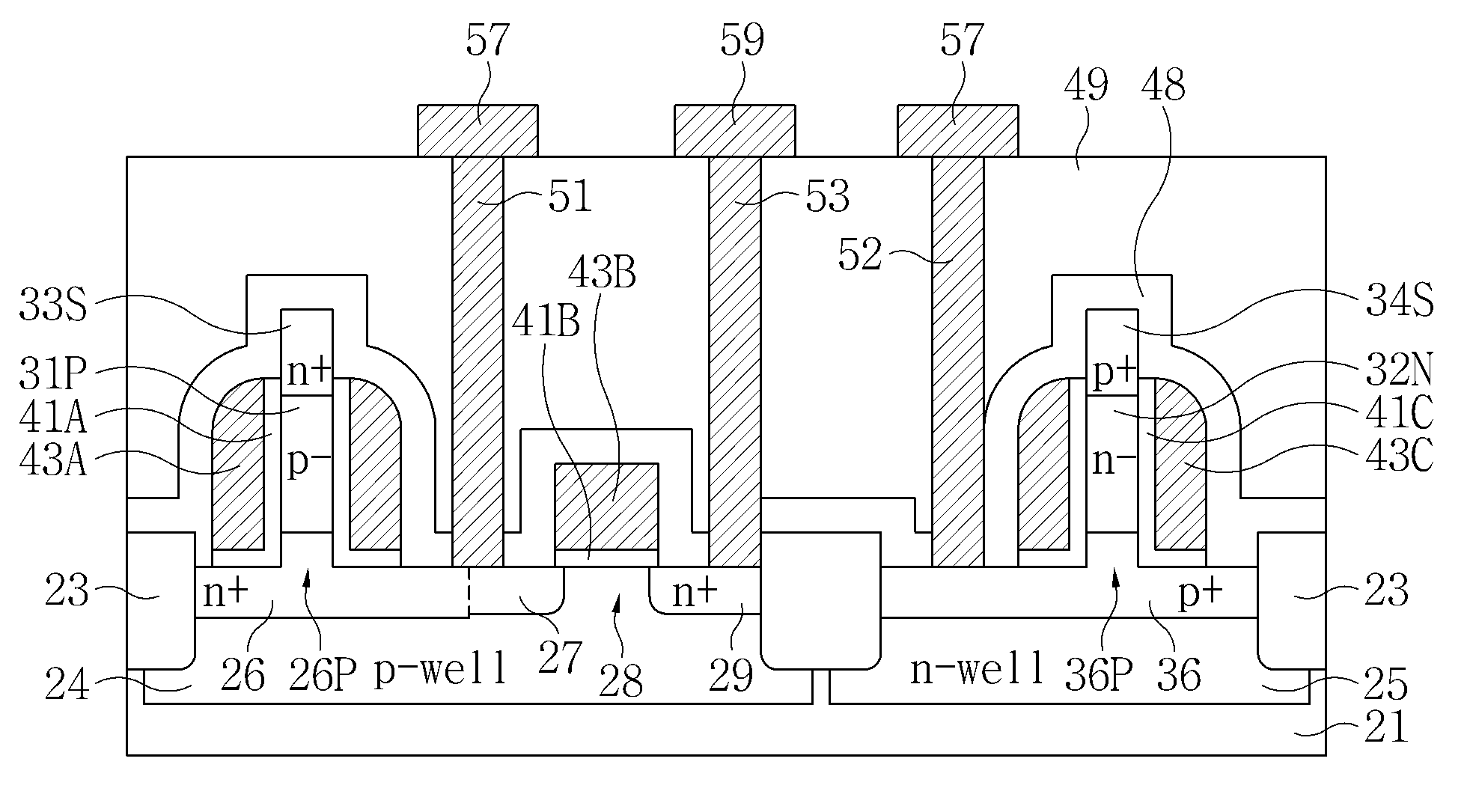
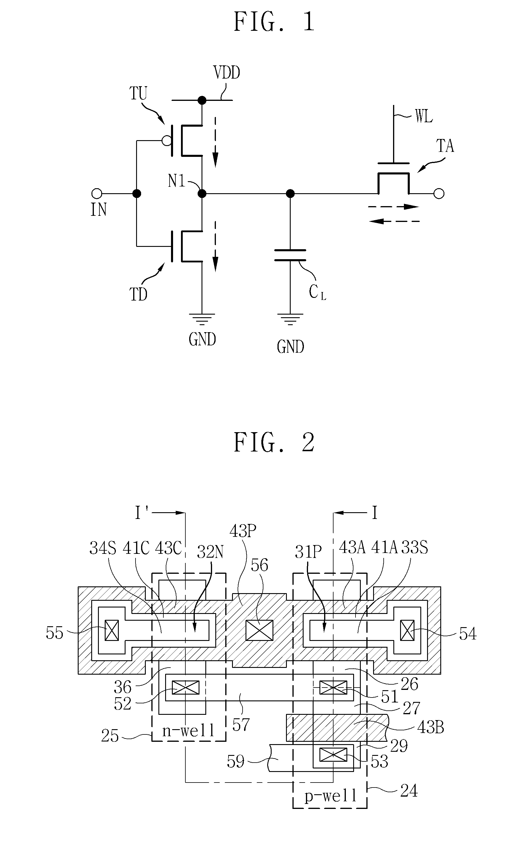
[0184]FIG. 1 is an equivalent circuit diagram of an electronic circuit including a complementary-metal-oxide-semiconductor (CMOS) inverter according to em...

embodiment 2

[0213]FIG. 4 is a cross-sectional view of a semiconductor device according to a second embodiment of the inventive concept.

[0214]Referring to FIG. 4, in this embodiment, a p-vertical channel region 31P and an n-source region 33S may be formed on an n-drain region 26. First insulating spacers 63 may be formed on sidewalls of the n-source region 33S. The n-drain region 26 may include an n-protrusion 26P that extends in the vertical direction. A first gate dielectric layer 41A and a first gate electrode 43A may be formed on sidewalls of the p-vertical channel region 31P.

[0215]The p-vertical channel region 31P may have a width in the horizontal direction that is less than that of the n-source region 33S. The n-protrusion 26P may have substantially the same width in the horizontal direction as that of the p-vertical channel region 31P.

[0216]An n-vertical channel region 32N and a p-source region 34S may be formed on a p-drain region 36. Second insulating spacers 64 may be formed on sidewa...

embodiment 3

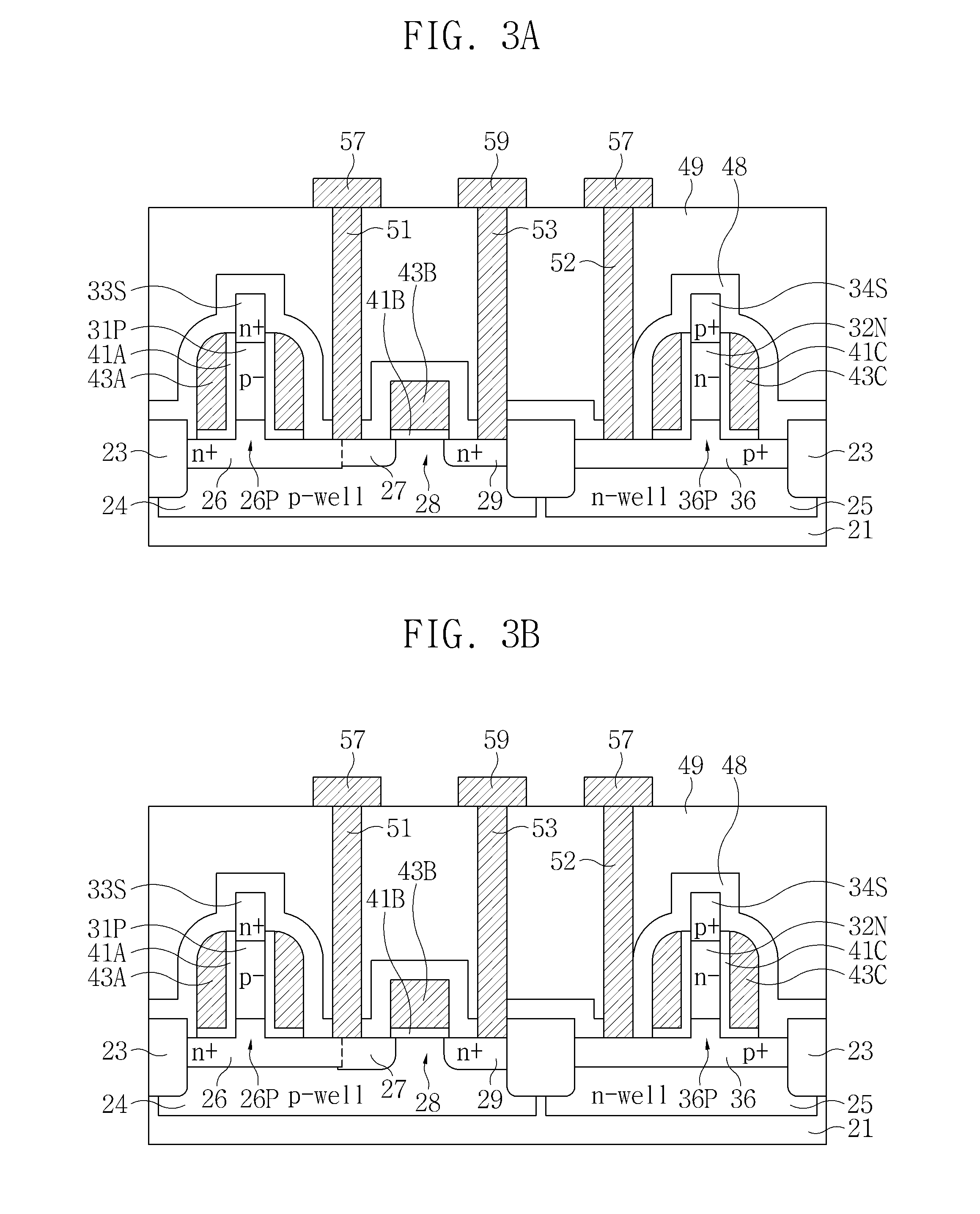
[0218]FIG. 5 is a cross-sectional view of a semiconductor device according to a third embodiment of the inventive concept.

[0219]Referring to FIG. 5, lightly doped regions 67 may be formed under an n-drain region 26, a first source / drain region 27, and a second source / drain region 29. The lightly doped impurity regions 67 may include impurities of the same conductivity type as the n-drain region 26, the first source / drain region 27, and the second source / drain region 29. The lightly doped regions 67 may include n-type impurities. A second gate electrode 66 may be formed between the first and second source / drain regions 27 and 29. A gate dielectric layer 65 may be formed between the second gate electrode 66 and a p-well 24. A channel region 68 may be defined in the p-well 24 by the first and second source / drain regions 27 and 29, the lightly doped regions 67, and the second gate electrode 66.

[0220]A bottom of the second gate electrode 66 may be formed at a lower level than the first a...


PUM


Abstract

In a semiconductor device, a vertical transistor comprises: a first diffusion region on a substrate; a channel region on the first diffusion region and extending in a vertical direction; a second diffusion region on the channel region; and a gate electrode at a sidewall of, and insulated from, the channel region. A horizontal transistor is positioned on the substrate, the horizontal transistor comprising: a first diffusion region and a second diffusion region on the substrate and spaced apart from each other; a channel region on the substrate between the first diffusion region and the second diffusion region; and a gate electrode on the channel region and isolated from the channel region. A portion of a gate electrode of the vertical transistor and a portion of the gate electrode of the horizontal transistor are at a same vertical position in the vertical direction relative to the substrate.

Description

CROSS-REFERENCE TO RELATED APPLICATION[0001]This application claims priority under 35 U.S.C. §119 to Korean Patent Application No. 10-2011-0058623 filed on Jun. 16, 2011, the disclosure of which is hereby incorporated by reference in its entirety.BACKGROUND[0002]1. Field[0003]Embodiments of the inventive concepts relate to semiconductor devices having a vertical transistor and a non-vertical transistor and methods of forming the same.[0004]2. Description of Related Art[0005]A vast amount of research has been conducted on various methods for embodying low-power semiconductor devices. With the growing tendency for MOSFETs to have channel lengths of about 100 nm or less, the fabrication of semiconductor devices having both a high driving current and a low off-leakage current has become increasingly difficult due to a phenomenon known in the industry as the short-channel effect. To overcome these limitations, fabrication techniques have been employed whereby devices having different thr...

Claims


Application Information

Patent Timeline
IPC IPC(8): H01L27/092
CPCH01L21/823487H01L27/1104H01L27/092H01L21/823885H10B10/12H01L29/7827
Inventor SUN, MIN-CHULPARK, BYUNG-GOOK
Owner SAMSUNG ELECTRONICS CO LTD
Why Eureka
Try Eureka