Transparent electroconductive film and organic electroluminescent device

a technology organic electroluminescent device, which is applied in the direction of non-metal conductors, conductors, synthetic resin layered products, etc., can solve the problems of insufficient sheet resistance and transmittance to achieve desirable levels of sheet resistance and transmittance, large process load, and deterioration of transparent electroconductive film transparency, electroconductivity and strength of film, and excellent emission uniformity, the effect of improving the degree of transparency

Inactive Publication Date: 2012-12-20
KONICA MINOLTA INC
View PDF10 Cites 3 Cited by
  • Summary
  • Abstract
  • Description
  • Claims
  • Application Information

AI Technical Summary

Benefits of technology

[0010]The present invention was conceived after considering the subjects described in the above. The present invention is to provide a transparent electroconductive film excellent in the transparency, electroconductivity, and strength of film, and less likely to degrade the transparency, electroconductivity, and strength of film even under high-temperature, high-humidity environments. The present invention is also to provide an organic EL device using the transparent electroconductive film, excellent in emission uniformity, less causative of degradation in the emission uniformity even under high-temperature, high-humidity environments, and have a long service life of emission.

Problems solved by technology

The transparent electrode has, however, been desired to disuse indium, since it is a rare metal and the price of which has been soaring.
The configuration, however, needs to smoothen irregularity of metal fine wire, causative of leakage of organoelectric devices, using a transparent electroconductive material composed of an electroconductive polymer or the like.
The electroconductive polymer film, however, shows absorption in the visible light region, so that thickening thereof considerably degrades the transparency of the transparent electroconductive film.
These techniques are, however, still insufficient to achieve desirable levels of sheet resistance and transmittance, and to achieve them at the same time.
The technique disclosed in JP-A-2011-96437 needs high temperature and long time for drying so as to fully proceed the crosslinking reaction, and this means a large load of processes.
Unreacted materials in the crosslinking reaction or eliminated products derived from the crosslinking reaction may adversely affect the transparent electrode and the organic EL device during storage, so that a desirable level of storability is not obtainable.
It is still also anticipated that a desired level of surface smoothness of the transparent electroconductive film is not obtainable if a polymer having a low glass transition point is used for the transparent electrode, and that performances of the transparent electrode and the organic EL device after environmental test may degrade.

Method used


Image

  • Transparent electroconductive film and organic electroluminescent device
  • Transparent electroconductive film and organic electroluminescent device
  • Transparent electroconductive film and organic electroluminescent device

Examples


example 1

Manufacturing of Transparent Electroconductive Film

[0130]

[0131]On one surface of the base where the first electroconductive layer was thus-formed by gravure printing and on the first electroconductive layer, coating liquid A described below was coated by extrusion, while adjusting the slit width of an extrusion head so as to give a dried film thickness of 300 nm, and the coated film was dried at 110° C. for 5 minutes. The second electroconductive layer, composed of the electroconductive polymer and the binder resin dispersible into aqueous solvent, was then formed thereon, and the obtained film was cut into 8×8 cm pieces. The obtained film was baked in an oven at 110° C. for 30 minutes, to thereby manufacture a transparent electroconductive film TC-101.

(Coating Liquid A)

[0132]Electroconductive polymer: PEDOT-PSS Clevios PH510 (solid content=1.89%, from H.C. Starck GmbH) 1.59 g

Binder: Polysol FP3000 (aqueous solution with a solid content of 54.4%) 0.13 g

Dimethyl sulfoxide (DMSO, one-...

example 2

Manufacturing of Organic EL Device

[0160]Each of the transparent electroconductive film bases manufactured in Example 1 was washed with ultra pure water, and cut into 30-mm square pieces so as to allow placement of 20-mm square tile-like transparent pattern at the center of each piece. Using each piece as an anode, an organic EL device was manufactured according to the procedures below. A hole transport layer and the layers stacked thereafter were formed by deposition. Organic EL devices OEL-201 to OEL-215 were manufactured using the transparent electroconductive films TC-101 to TC-115, respectively.

[0161]Necessary amounts of constitutive materials for composing the individual layers (Compounds 1-6 described below, CsF and Al) were respectively filled in evaporation crucibles of a deposition apparatus. The evaporation crucibles employed herein were made of molybdenum or tungsten suitable for electric resistance heating.

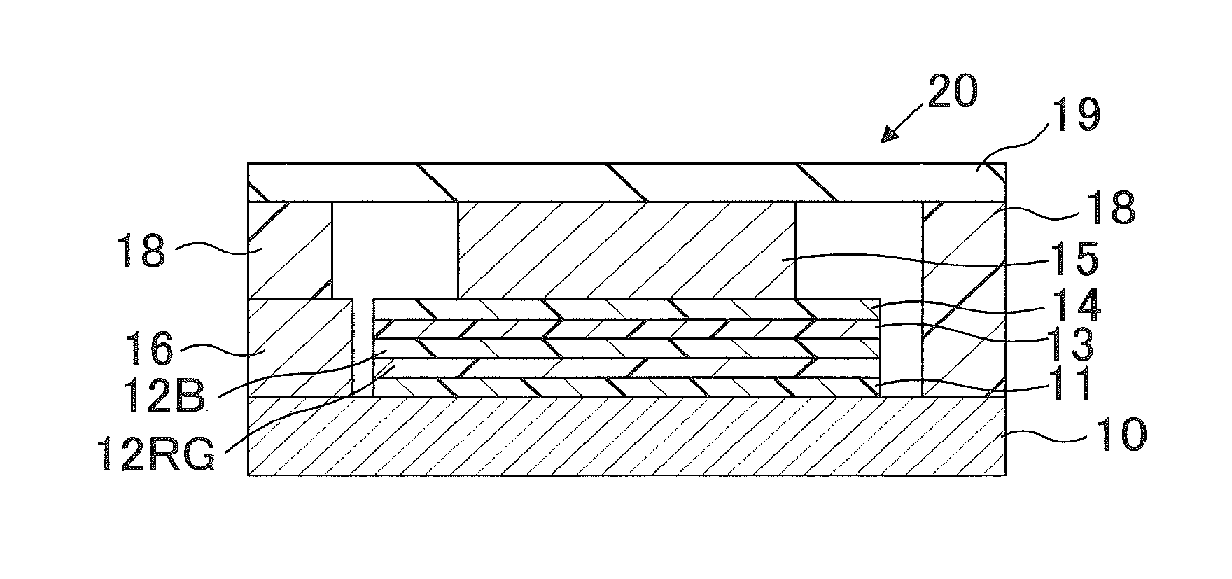
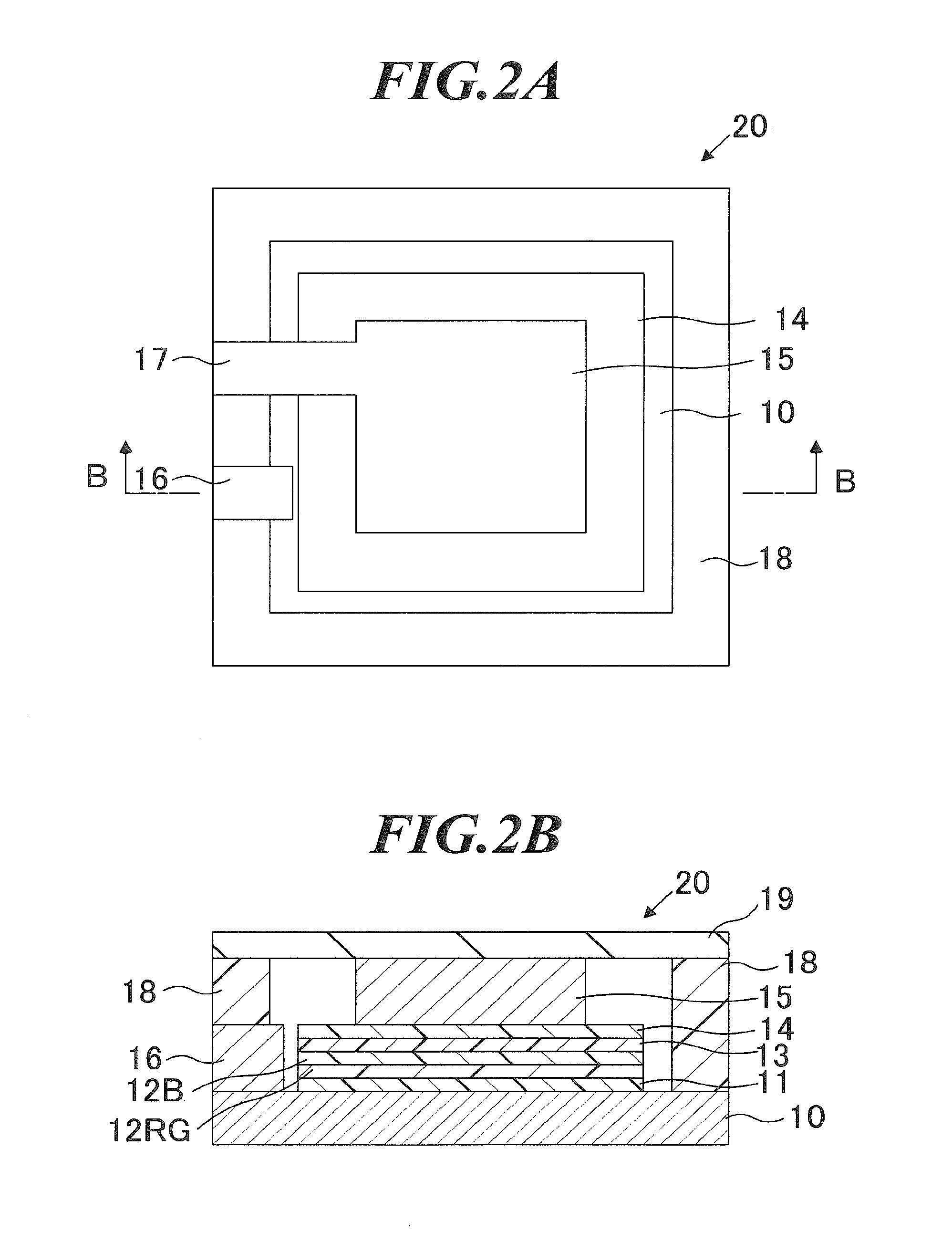
[0162]FIG. 2A is a top view of an exemplary organic EL device of ...


PUM

PropertyMeasurementUnit
glass transition pointaaaaaaaaaa

Abstract

Provided is a transparent electroconductive film. The film includes a transparent electroconductive layer. The layer contains an electroconductive polymer and a self-dispersing polymer dispersible into aqueous solvent. The self-dispersing polymer has a dissociable group, and has a glass transition point of 25° C. or higher and 80° C. or lower.

Description

CROSS-REFERENCE TO RELATED APPLICATION[0001]The present U.S. patent application claims a priority under the Paris Convention of Japanese patent application No. 2011-134872 filed on Jun. 17, 2011, which shall be a basis of correction of an incorrect translation, and is incorporated by reference herein.BACKGROUND OF THE INVENTION[0002]1. Technical Field[0003]The present invention relates to a transparent electroconductive film successfully applicable to various fields including liquid crystal display device, organic electroluminescent device, inorganic electroluminescent device, solar battery, electromagnetic shield, electronic paper, touchscreen and so forth, and an organic electroluminescent device (also referred to as “organic EL device”, hereinafter) having the transparent electroconductive film.[0004]2. Related Art[0005]With the recent growing demand for thin TV set, display technologies of various styles, including those making use of liquid crystal, plasma, organic electrolumin...

Claims


Application Information

Patent Timeline
Patent Type & Authority Applications(United States)
IPC IPC(8): H01B1/12B32B3/10B32B27/18
CPCH01B1/02H01B1/026H01B1/127H01B1/128H01L51/442H01L51/5206Y10T428/31533H01L51/5212Y10T428/24322Y10T428/24868Y10T428/24917H10K30/82H10K50/81H10K50/814
Inventor NAKAMURA, KAZUAKISUZUKI, TAKAYUKI
Owner KONICA MINOLTA INC
Why Eureka
Try Eureka