Organic light-emitting diode and flat display device including the same

a technology of light-emitting diodes and display devices, which is applied in the direction of luminescent compositions, thermoelectric devices, chemistry apparatuses and processes, etc., can solve the problems of unsatisfactory luminance, efficiency, driving stability, etc., and achieve the effect of reducing the bulk resistance of the transport layer, reducing the interface resistance, and increasing the number of free holes

Active Publication Date: 2012-12-27
SAMSUNG DISPLAY CO LTD
View PDF11 Cites 31 Cited by
  • Summary
  • Abstract
  • Description
  • Claims
  • Application Information

AI Technical Summary

Benefits of technology

[0009]Aspects of embodiment of the present invention are directed toward an organic light-emitting diode in which the structure and material of a hole transport layer are changed to reduce an interface resistance between an electrode and an organic layer, increase the number of free holes of the hole transport layer and reduce a bulk resistance of the hole transport layer, whereby the organic light-emitting diode has enhanced performances, and a flat display device including the same.

Problems solved by technology

An OLED has not had fully satisfactory characteristics in terms of luminance, efficiency, driving stability, lifetime, and the like, and thus there is an urgent need for development of various improvement technologies.

Method used


Image

  • Organic light-emitting diode and flat display device including the same
  • Organic light-emitting diode and flat display device including the same
  • Organic light-emitting diode and flat display device including the same

Examples


example 1

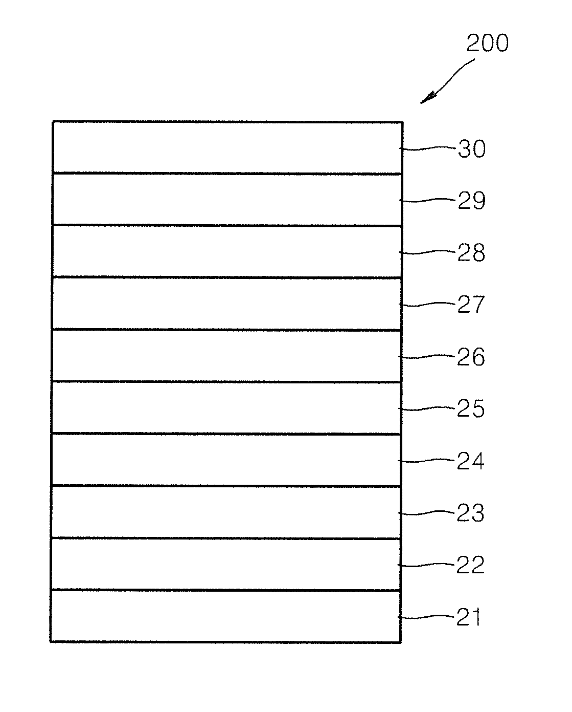
[0112]As an anode, 15 Ω / cm2 (1200 Å) of an ITO glass substrate from Corning Co., Ltd. was cut to a size of 50 mm×50 mm×0.7 mm, was ultrasonically washed with isopropyl alcohol and pure water each for 5 minutes, and then washed with UV ozone for 15 minutes.

[0113]A first mixing layer formed by doping Compound 105 represented above with a compound represented by Formula 20A where each of R103 and R109 is F was formed to a thickness of 100 Å on the ITO glass substrate, wherein the amount of the compound of Formula 20A is 1 part by weight based on 100 parts by weight of the first mixing layer. A first hole transport layer was formed to a thickness of 650 Å on the first mixing layer by using Compound 105 above.

[0114]A second mixing layer formed by doping Compound 105 represented above with a compound represented by Formula 20A where each of R103 and R109 is F was formed to a thickness of 100 Å on the first hole transport layer, wherein the amount of the compound of Formula 20A is 1 part b...

example 2

[0117]An organic light-emitting diode was manufactured in the same manner as in Example 1, except that the amount of the compound represented by Formula 20A where each of R103 and R109 is F, was 3 parts by weight based on 100 parts by weight of the first mixing layer.


PUM


Abstract

An organic light-emitting diode including a first electrode; a second electrode facing the first electrode; an emission layer interposed between the first electrode and the second electrode; a first hole transport layer including a first hole transporting compound; a second hole transport layer including a second hole transporting compound, the first and second hole transport layers being interposed between the first electrode and the emission layer; an electron transport layer interposed between the emission layer and the second electrode; a first mixing layer interposed between the first electrode and the first hole transport layer, contacting the first hole transport layer, and including the first hole transporting compound and a first cyano group-containing compound; and a second mixing layer interposed between the first electrode and the second hole transport layer, contacting the second hole transport layer, and including the second hole transporting compound and a second cyano group-containing compound.

Description

CROSS-REFERENCE TO RELATED PATENT APPLICATION[0001]This application claims priority to and the benefit of Korean Patent Application No. 10-2011-0059170, filed on Jun. 17, 2011, in the Korean Intellectual Property Office, the disclosure of which is incorporated herein in its entirety by reference.BACKGROUND[0002]1. Field[0003]The following description relates to an organic light-emitting diode and a flat display device including the same, and more particularly, to an organic light-emitting diode including a multi-layered hole transport layer, wherein the multi-layered hole transport layer is doped with a cyano group-containing compound and a flat display device including the same.[0004]2. Description of Related Art[0005]Organic light-emitting diodes (OLEDs), which are self-emitting devices, have advantages such as a wide viewing angle, excellent contrast, quick response, high brightness, and excellent driving voltage characteristics, and can provide multicolored images.[0006]A genera...

Claims


Application Information

Patent Timeline
Patent Type & Authority Applications(United States)
IPC IPC(8): H01L51/54
CPCH01L51/0051H01L51/0054H01L51/006H01L51/5064H01L51/5008H01L51/506H01L51/0061H10K85/611H10K85/622H10K85/636H10K85/633H10K30/865H10K50/155H10K50/156C09K11/06H10K50/00
Inventor SONG, WON-JUNPARK, MIE-HWALEE, KWAN-HEEKHO, SAM-ILLEE, SUN-HEE
Owner SAMSUNG DISPLAY CO LTD
Why Eureka
Try Eureka