Touch sensitive film and a touch sensing device

Active Publication Date: 2012-12-27
CANATU OY
View PDF12 Cites 19 Cited by
  • Summary
  • Abstract
  • Description
  • Claims
  • Application Information

AI Technical Summary

Benefits of technology

[0027]In a preferred embodiment of the present invention, the sheet resistance is within a range of 5 to 100 kΩ, preferably within a range of 10 to 50 kΩ, most preferably in the range of 10 to 20 kΩ. These are even more preferred values for maximizing the sensitivity and touch location resolution performance of the touch sensitive film. Increasing the resistivity increases the noise in the measurements as well as different electromagnetic interference effects, which can set an upper limit for the sheet resistance according to the overall conditions of each specific application.
[0057]As well known in the art, haptic feedback can very significantly improve the user experience of touch sensing device. In known touch sensing devices configured for producing haptic feedback via the conductive layer, high voltages are typically used in generating the haptic feedback effect. Low resistances of the conductive layers of the known devices then lead to high currents through the conductive layer. High currents can induce various problems in the device, for instance excessive power demands or electromagnetic interference with the display or touch sensing circuitries. With the resistivity of the conductive layer in the touch sensing region according to the present invention, the current will be clearly lower, thereby reducing those problems particularly in the case of providing the haptic feedback via the conductive layer.

Problems solved by technology

One particularly challenging issue is detection of multiple simultaneous touches which, on the other hand, often is one of the most desired properties of the touch sensing devices.
Complex sensing electrode configurations and high numbers of single sensing electrode elements complicates the manufacturing process as well as the measurement electronics of the touch sensing device.
Visibility of the touch sensitive film to the user of e.g. an LCD (Liquid Crystal Display), an OLED (Organic Light Emitting Diode) display, or an e-paper (electronic paper) display seriously deteriorates the user experience.
However, from the visibility point of view, they are far from an ideal solution.
The problem is emphasized as the sensing electrode patterning becomes more complicated.
However, also this document involves the common problem of very complex electrode and measurement circuitry configurations.

Method used


Image

  • Touch sensitive film and a touch sensing device
  • Touch sensitive film and a touch sensing device
  • Touch sensitive film and a touch sensing device

Examples


Embodiment Construction

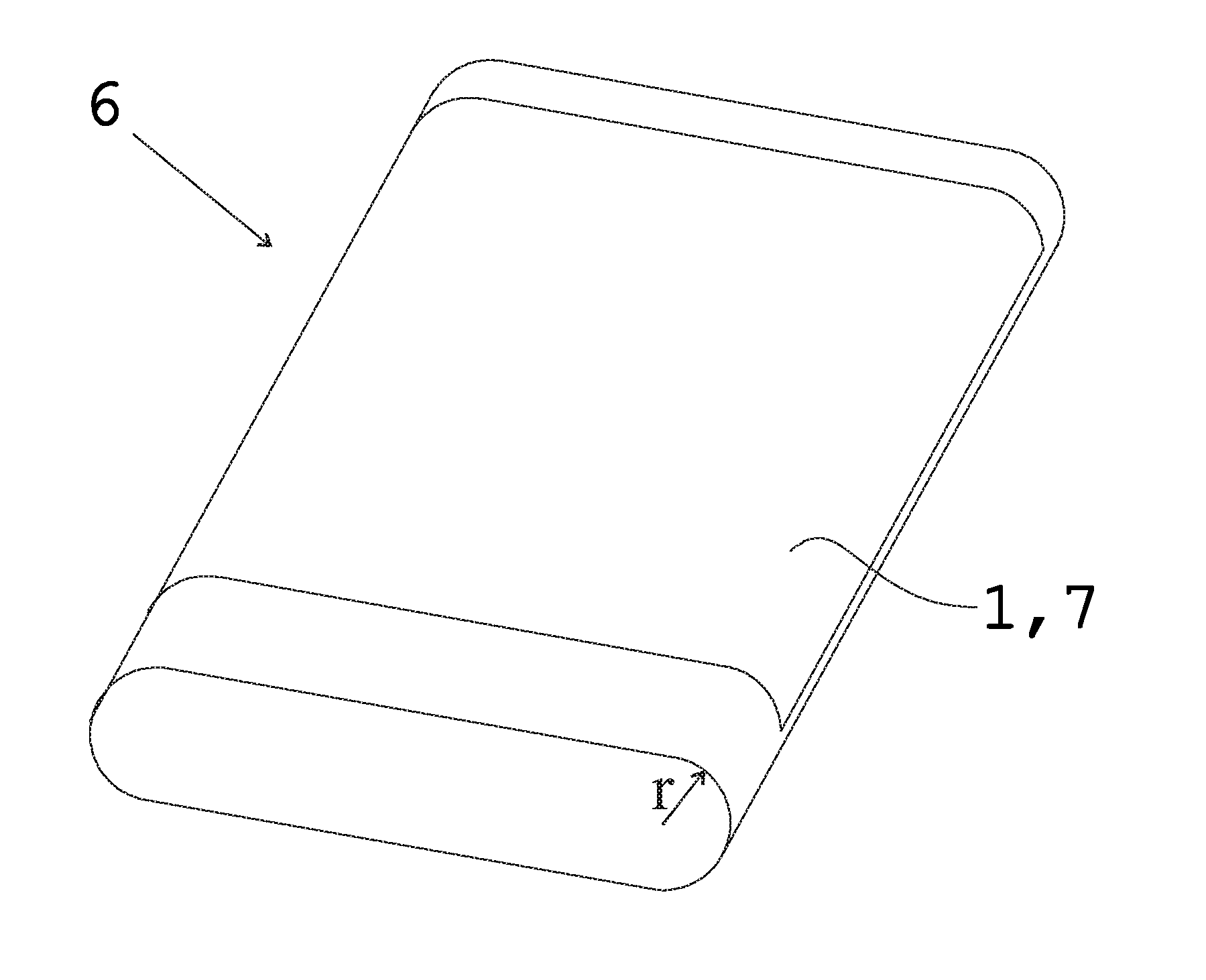
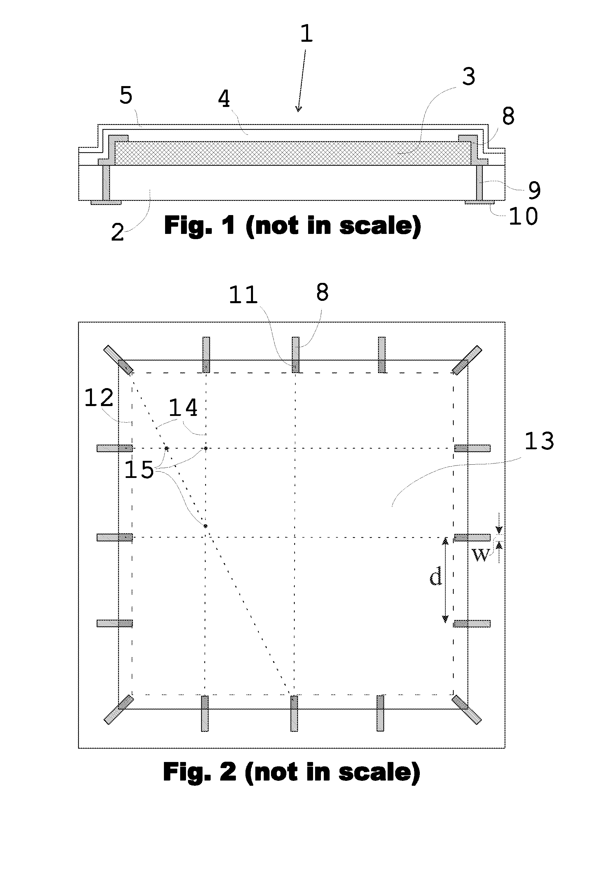
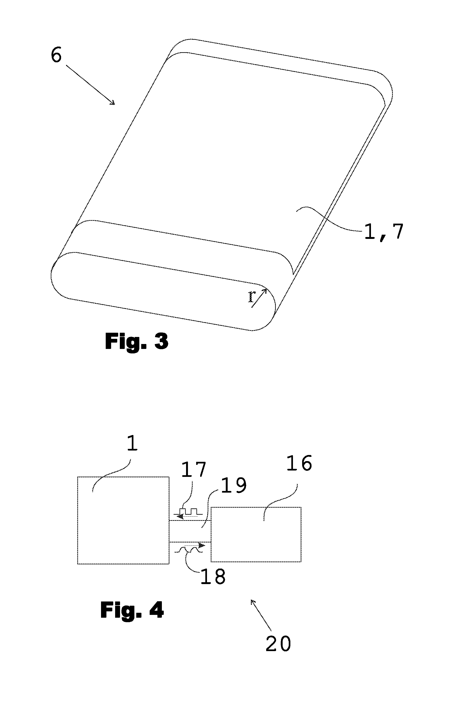
[0066]The touch sensitive film 1 shown in FIG. 1 comprises a substrate 2 and a conductive layer 3, the latter being formed of networks of HARM (High Aspect Ratio Molecule) structures, e.g. carbon nanotubes and / or carbon NANOBUDs. The substrate can be made of, for example, polyethylene terephthalate PET. In addition to the HARMS networks, the conductive layer can also comprise suitable species chemically bonded to, physically absorbed on, or otherwise combined with the layer as a dopant to adjust the sheet resistance of the layer. The sheet resistance of the conductive layer 3 is above 3 kΩ and preferably in the range of 3 to 40 kΩ, e.g. 25 kΩ. As described earlier in this document, these kinds of resistance range and composition of the conductive layer allow a superior touch detection performance of a touch sensing device utilizing such a touch sensitive film. The conductive layer of FIG. 1 can have a thickness of e.g. 5 nm.

[0067]The touch sensitive film shown in FIG. 1 and explaine...


PUM


Abstract

A capacitive touch sensitive film comprises a conductive layer having a sensing region. According to the present invention, the sheet resistance of the conductive layer in the sensing region is higher than or equal to 3 kΩ.

Description

FIELD OF THE INVENTION[0001]The present invention relates to touch sensitive films, and touch sensing devices utilizing touch sensitive films.BACKGROUND OF THE INVENTION[0002]User interfaces for different kinds of electrical apparatuses are nowadays more and more often realized by means of different types of touch sensing devices based on touch sensitive films instead of conventional mechanical buttons. Different kinds of touch pads and touch screens of e.g. mobile phones, portable computers and similar devices are well known examples of these. In addition to the sophisticated and even luxurious user experience achievable, touch sensing devices based on touch sensitive films also provide a superior freedom to the designers continuously trying to find functionally more versatile, smaller, cheaper, lighter, and also visually more attractive devices.[0003]A key element in such touch sensing devices is a touch sensitive film comprising one or more conductive layers configured to serve a...

Claims


Application Information

Patent Timeline
IPC IPC(8): H03K17/975G06F3/041
CPCG06F3/044G06F3/0444G06F2203/04102G06F2203/04103G06F2203/04104G06F3/04164G06F3/04166G06F3/0446G06F3/0443
Inventor MIKLADAL, BJORN FRIOURBROWN, DAVID P.AITCHISON, BRADLEY J.
Owner CANATU OY
Why Eureka
Try Eureka