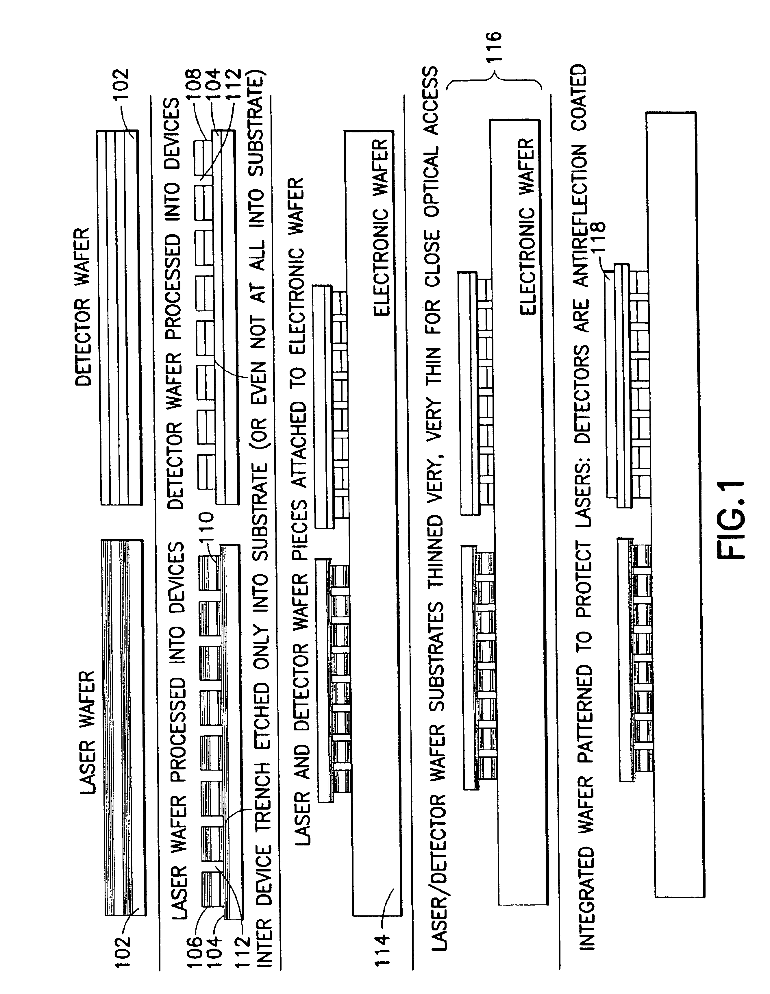
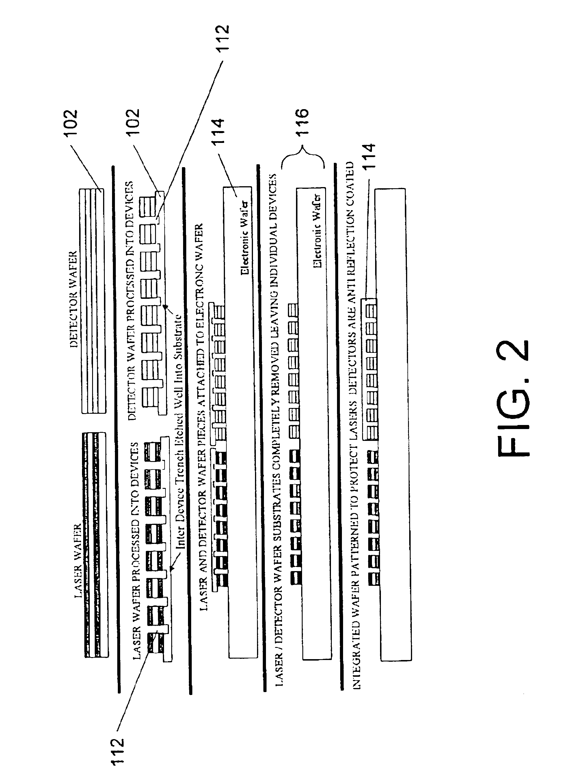
1 and FIG. 2 make it possible to get optical fibers or optical lenses close enough to the devices to capture the appropriate light without allowing light coming from, or going to, adjacent devices to affect any of those adjacent devices, a problem known as “
crosstalk”.
Both of these techniques however, characteristically create opto-electronic chips that have heat dissipation problems during use and leave the individual devices more sensitive to thermal and mechanical stresses produced during the manufacturing process, thereby reducing individual device lifetimes and, accordingly, decreasing yields and overall chip life.
Moreover, for the approach of both FIG. 1 (where the substrate is extremely thin) and FIG. 2 (where the substrate is completely removed), stresses experienced by the devices are primarily transferred to the very thin optical device layer which is the structurally weakest part of the device.
However, typically electrical and optical chips are not designed concurrently, even if they are designed and fabricated within the same organization.
Thus, even with a single manufacturer, unless there is close coordination within the organization with regard to both the optical and electronic chip design, a lack of correspondence between contact pads on each can easily occur—particularly where one or both are also designed with sales to third parties in mind or integration with devices from other sources is contemplated.
Moreover, subsequent improvements or changes in the design of either may necessitate altering the location of the contact pads, thereby introducing a pad misalignment where none previously existed.
Even worse, if the electronic chip is designed to be used with a variety of different optical chips, but the optical chips are commodity stock obtained from third parties (for example, chips containing: topside emitting
vertical cavity lasers, bottom emitting
vertical cavity lasers, distributed feedback (DFB) or
distributed Bragg reflector (DBR) lasers (which each have better
chirp and linewidth characteristics for long distance applications), topside receiving detectors or bottom receiving detectors) that are
mass manufactured for distribution to multiple unrelated users, it is unlikely that the pads on the optical devices will all be located in the same place, even if they are otherwise compatible with the electronic chip.
This presents a problem in that it limits the ability to “mix-and match” devices.
Moreover, if a chip is designed with connection to a particular other chip in mind, and subsequent events create a need to use a different device with a different contact placement, all the planning and coordination done for the
original device will be irrelevant to the
new device.
In addition, in some cases it is sometimes desirable to coat some of the devices, specifically the detectors, with an AR
coating.
As a result, at a minimum it will detrimentally affect the lasing action of the laser, if not prevent it from lasing altogether.
The protection or disparate treatment of the various different devices on the
wafer requires extra
processing steps, which costs time, and hence increases the cost of
processing.
It also introduces the possibility of damaging the protected devices.
In addition disparate treatment of devices causes other
processing problems when the processing must be performed on a chip having electrical contact pads in the same area.
For example, if a chip has
electrical contacts near the devices and
electroplating,
electroless plating, thermal evaporates, e-beam evaporated or
sputtering techniques are used to place solder on the contact pads, the height of the resulting solder bumps, renders it difficult to pattern areas to protect lasers from AR coating because the solder bumps are much taller than the optical devices.
Prior art lacks a way to eliminate the need to pattern a protective layer over the lasers while allowing the entire wafer (i.e. lasers and detectors) to be AR coated.

