

Spin device, and operating method therefor and manufacturing method therefor
- Summary
- Abstract
- Description
- Claims
- Application Information
AI Technical Summary
Benefits of technology
Problems solved by technology
Method used
Image

Examples
embodiment
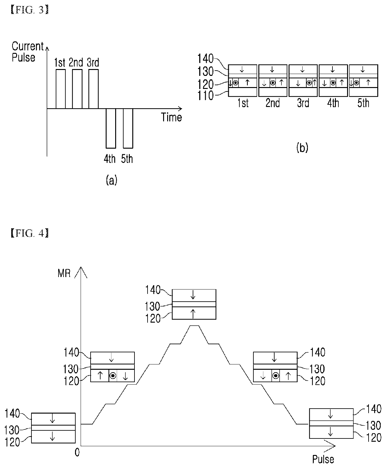
[0062]The present invention discloses a neuron device and synapse device for application to a neuromorphic computer and the like, and neuromorphic device using movement of magnetic domain wall by spin orbit torque so that synaptic operation or neuron operation similar to living organisms is implemented.
[0063]Generally, when a CMOS synapse device or a CMOS neuron device is fabricated, the size of the CMOS synapse device or the CMOS neuron device is large, integration is difficult, and the manufacturing process is complicated, resulting in a high production cost. The best way to solve such a problem is to use a spin orbit torque (SOT) and to manufacture a device capable of controlling the magnetic domain wall by using the SOT.
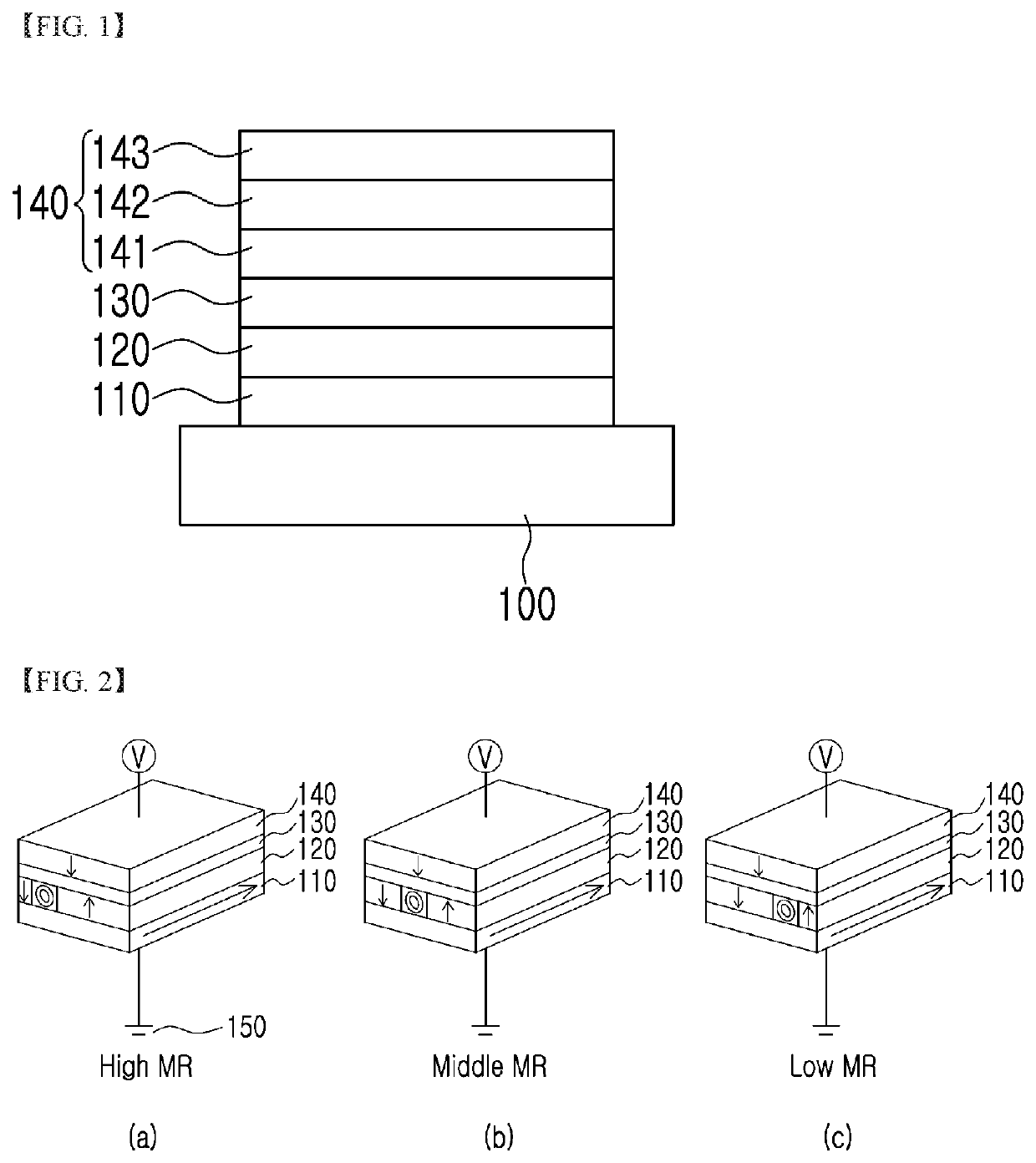
[0064]FIG. 1 is a cross-sectional view of a spin device driven by using a spin orbital torque (SOT) according to a preferred embodiment of the present invention.
[0065]Referring to FIG. 1, an electrode 110 is formed on a substrate 100. The electrode 110 is made of...
production example 1
[0098]For experimental investigation, the spin device is fabricated with the following structure. Si is used as a substrate, and SiO2 is formed to a thickness of 120 nm on Si substrate. Subsequently, Ta is formed to thickness of 2 nm as the electrode 110, and then the free layer 120 is formed of Co0.4Fe0.55B0.05 on the electrode 110.
[0099]Further, MgO is formed to thickness of 2 nm as the tunnel barrier layer 130 sequentially on the free layer 120, and Fe is formed to a thickness of 4 nm as the first pinned layer 141 on the tunnel barrier layer 130.
production example 2
[0132]The neuron spin device as shown in FIG. 11 is manufactured. In the neuron spin device, a first non-magnetic layer 320 is formed between the pinned layer 310 and the first multi-layer 330, and a second non-magnetic layer 340 is formed between the first multi-layer 330 and the second multi-layer 350. The pinned layer 310 is disposed on the tunnel barrier layer 240.
[0133]The first multi-layer 330 and the second multi-layer 350 are each formed by alternately stacking Pd and Co, and the number of layers of the first multi-layer 330 is smaller than that of the second multi-layer 350.
[0134]Si is prepared as a substrate 210 and tungsten (W) is formed to a thickness of 10 nm on the substrate 210 as an electrode 220. Then, the free layer 230 is formed to thickness of 5 nm with CoFeB. On the free layer 230, MgO is formed to 3 nm thickness as the tunnel barrier layer 240.
[0135]Furthermore, Ta is formed to a thickness of 3 nm for the first non-magnetic layer 320, and Ru is formed to a thic...
PUM
 Abstract
Description
Claims
Application Information