Chip type laminated capacitor

Active Publication Date: 2012-12-27
SAMSUNG ELECTRO MECHANICS CO LTD
View PDF0 Cites 14 Cited by
  • Summary
  • Abstract
  • Description
  • Claims
  • Application Information

AI Technical Summary

Benefits of technology

[0012]An aspect of the present invention provides a chip type laminated capacitor having reduced acoustic noise even in the case that a permittivity of a dielectric layer is lowered and a thickness thereof is remarkably reduced.

Problems solved by technology

These vibrations may be excessive in the case that the permittivity of the dielectric layer is high, when the size of the chip is relatively large, based on the same capacitance.
That is, when the resonance generated by the vibrations of the circuit board is in a range of an audible frequency (20 to 20,000 Hz), the sound of the vibrations in the circuit board may give a person an unpleasant feeling, wherein the vibration sound is referred to as acoustic noise.
Acoustic noise generated due to a piezoelectric phenomenon in a laminated ceramic capacitor using a ferroelectric material therefore causes serious defects in some electronic devices.
The sound of the vibrations may be a factor in noise generation in electronic devices equipped with the laminated ceramic capacitor.

Method used


Image

  • Chip type laminated capacitor
  • Chip type laminated capacitor
  • Chip type laminated capacitor

Examples


experimental example

[0107]The laminated ceramic capacitor according to Examples of the present invention and Comparative Examples was manufactured.

[0108]The plurality of ceramic green sheets manufactured to have a thickness of 3.9 μm by applying and drying the slurries formed including the powder such as barium titanate (BaTiO3), and the like, to the carrier film was prepared.

[0109]Next, the inner electrode was formed by applying the conductive paste for the nickel inner electrode to the ceramic green sheet using the screen for forming the patterns of which the margins are asymmetric on the ceramic green sheet.

[0110]The ceramic green sheets were laminated in 370 layers and the laminate was subjected to the isostatic pressing under the pressure condition of 1000 kgf / cm at 85° C. The pressed ceramic laminate was cut in an individual chip form and the cut chip was subjected to a debinder while being maintained at 230° C. for 60 hours under the atmosphere.

[0111]Thereafter, the ceramic laminate was fired in...

modified example

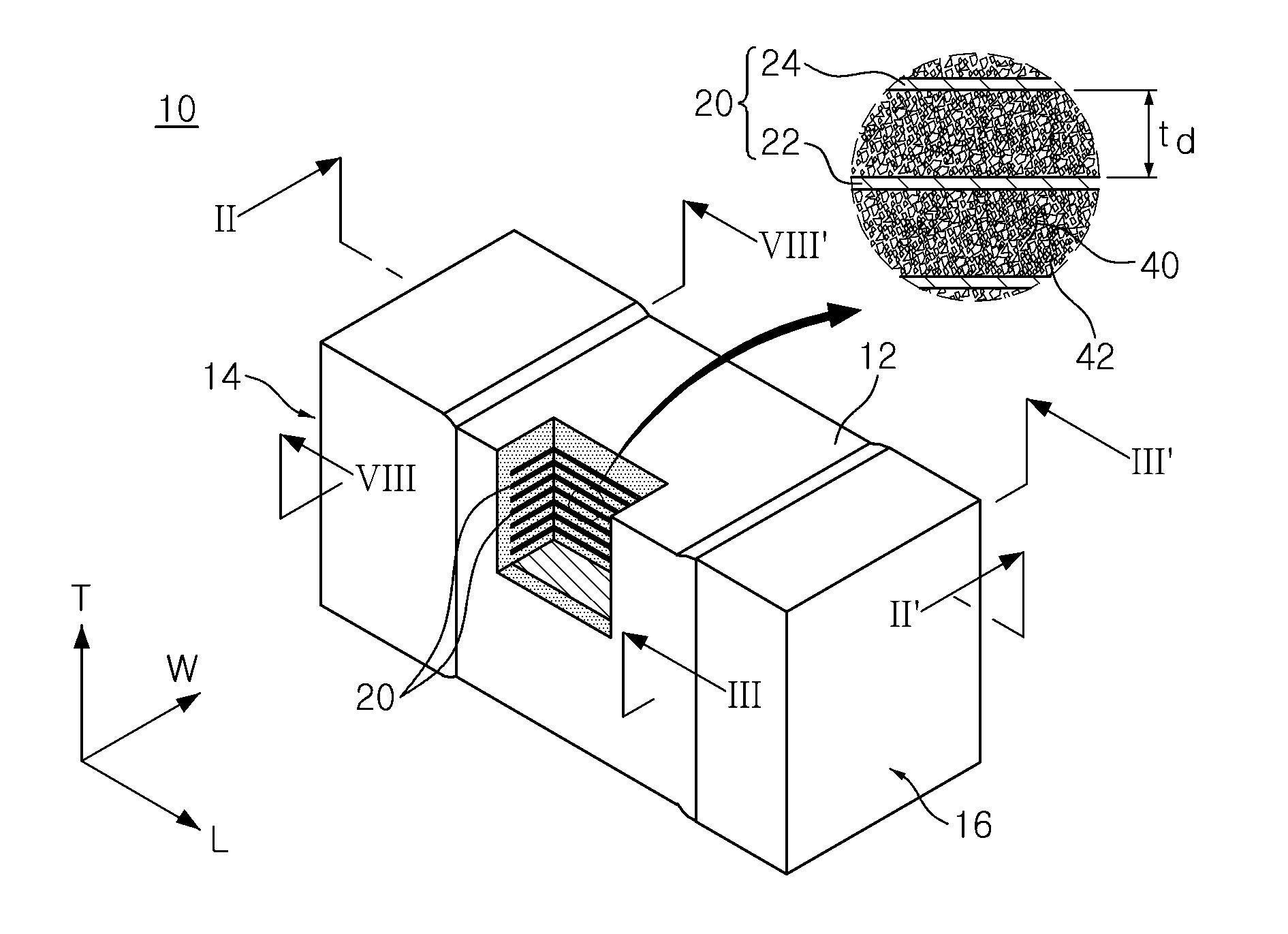
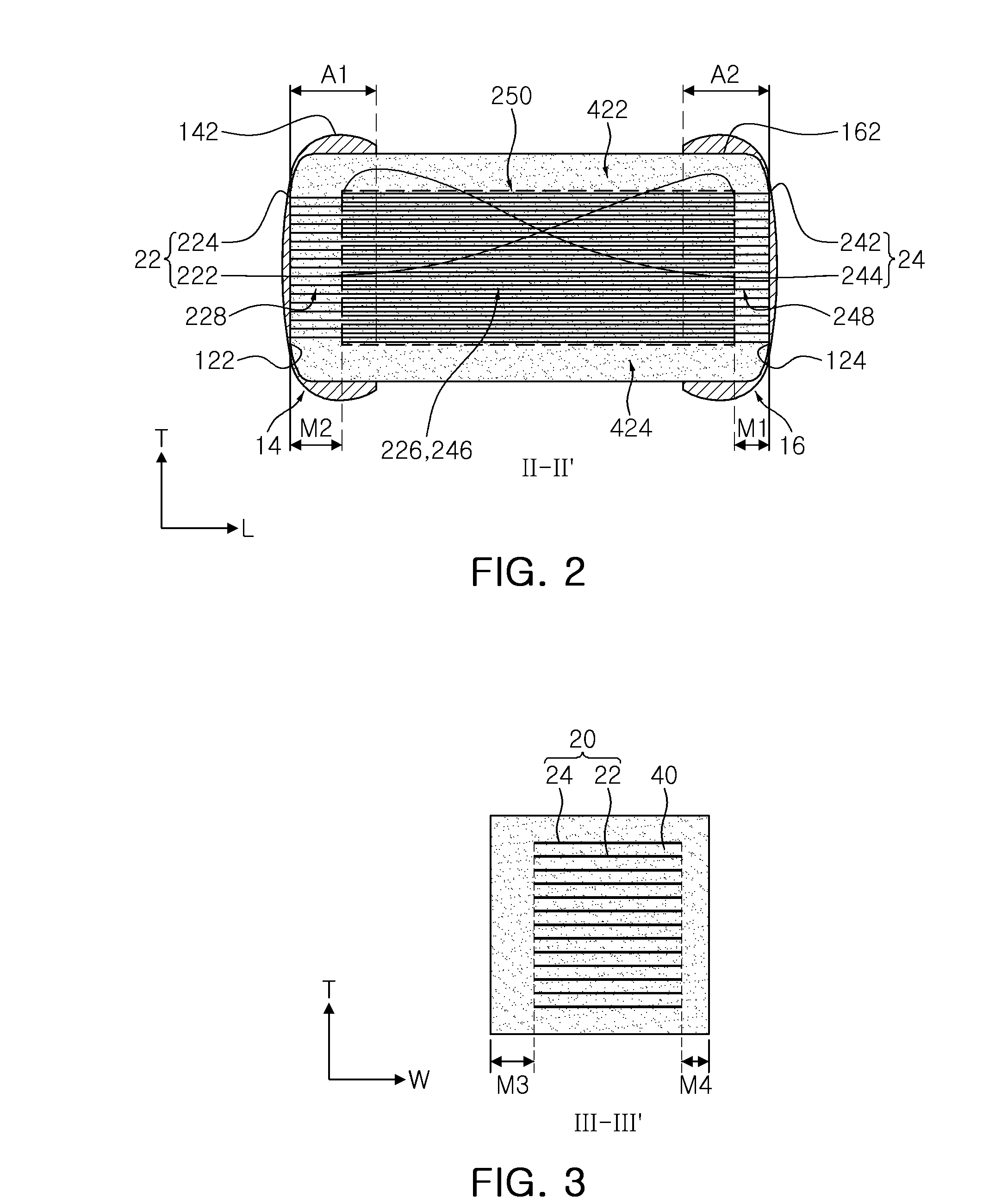
[0128]FIG. 5 is a plan view schematically showing a first embodiment of a shape in which inner electrodes formed on a dielectric layer are laminated and FIG. 8 is a cross-sectional view taken in direction W-T of a shape in which inner electrodes of FIG. 5 are led and is a cross-sectional view taken along line VIII-VIII′ of FIG. 1, where outer electrodes are removed.

[0129]FIG. 6 is a plan view schematically showing a second embodiment of a shape in which inner electrodes formed on a dielectric layer are laminated and FIG. 9 is a cross-sectional view taken in direction W-T of a shape in which the inner electrodes of FIG. 6 are led and is a cross-sectional view taken along line VIII-VIII′ of FIG. 1, where outer electrodes are removed.

[0130]In addition, FIG. 7 is a plan view schematically showing a third embodiment of a shape in which inner electrodes formed on a dielectric layer are laminated and FIG. 10 is a cross-sectional view taken in direction W-T of a shape in which the inner ele...


PUM

PropertyMeasurementUnit
Fractionaaaaaaaaaa
Thicknessaaaaaaaaaa
Lengthaaaaaaaaaa

Abstract

There is provided a chip type laminated capacitor including: a ceramic body formed by laminating a dielectric layer having a thickness equal to 10 or more times an average particle diameter of a grain included therein and being 3 μm or less; first and second outer electrodes; a first inner electrode having one end forming a first margin together with one end surface of the ceramic body at which the second outer electrode is formed and the other end leading to the first outer electrode; and a second inner electrode having one end forming a second margin together with the other end surface of the ceramic body at which the first outer electrode is formed and the other end leading to the second outer electrode, wherein the first and second margins have different widths under a condition that they are 200 μm or less.

Description

CROSS-REFERENCE TO RELATED APPLICATIONS[0001]This application claims the priority of Korean Patent Application No. 10-2011-0061345 filed on Jun. 23, 2011, in the Korean Intellectual Property Office, the disclosure of which is incorporated herein by reference.BACKGROUND OF THE INVENTION[0002]1. Field of the Invention[0003]The present invention relates to a chip type laminated capacitor capable of reducing an acoustic noise while implementing miniaturization and high capacitance.[0004]2. Description of the Related Art[0005]With an increased demand for small-sized and multi-functional electronics, the demand for a compact, high-capacitance chip type laminated capacitors embedded in electronics has also increased.[0006]In order to reduce the size of a chip type laminated capacitor and increase the capacitance thereof, there is a need to use a high-K material, for example, barium titanate, as a ceramic material forming a dielectric layer. When AC and DC voltages are applied to the chip t...

Claims


Application Information

Patent Timeline
IPC IPC(8): H01G4/12
CPCH01G4/30H01G2/065H01G4/005H01G4/232H01G4/1272H01G4/228H01G4/12
Inventor AHN, YOUNG GHYULEE, BYOUNG HWAPARK, MIN CHEOLSONG, YOUNG HOONLEE, MI HEE
Owner SAMSUNG ELECTRO MECHANICS CO LTD
Why Eureka
Try Eureka