

Capping Coating for 3D Integration Applications
a technology of 3d integration and coating, applied in the field of circuit components integration, can solve the problems of difficult cleaning, limited pattern solution, worsening situation,
- Summary
- Abstract
- Description
- Claims
- Application Information
AI Technical Summary
Benefits of technology
Problems solved by technology
Method used
Image

Examples
Embodiment Construction
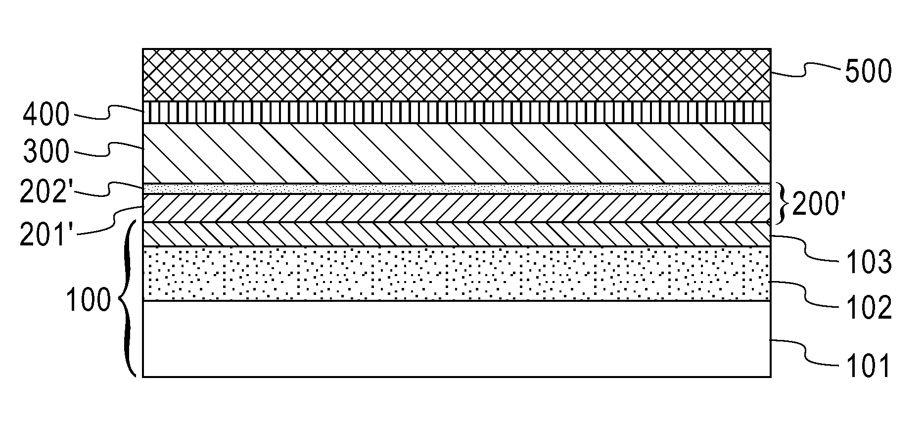
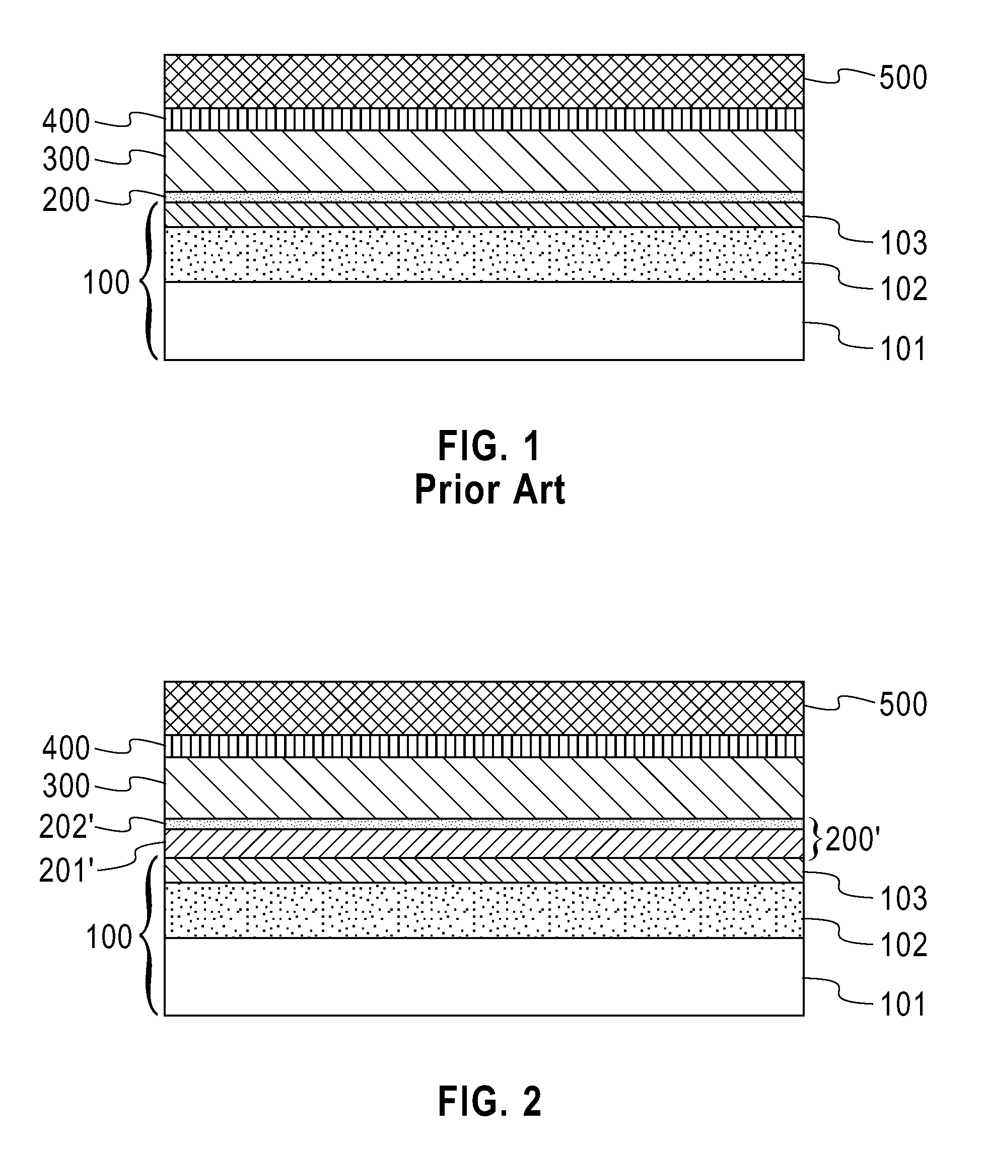
[0043]The present invention relates to a method for manufacturing 3D integrated structures based on an assembly approach in which a layer-to-be transferred is coated with a bi-layer capping stack, a polyimide layer, and an adhesive layer. That structure is then bonded to a glass carrier-wafer and upon removal of the bulk silicon, it is transferred to a new circuit, and attached to this new circuit using bonding techniques such as, for example, adhesive bonding. In the subsequent step, the glass layer is released (for example, by laser ablation), and the residual polyimide layer is removed by plasma ashing using oxygen.
[0044]The aforementioned protecting capping stack is comprised of two layers including a first layer of silicon nitride and a second layer of an amino silane deposited over the whole area of the wafer. Such a bi-layer cap provides not only protection from both Cu and oxygen diffusion, but it presents a SiCMOS-compatible and reliable solution for use in the 3D applicati...
PUM
 Abstract
Description
Claims
Application Information