Group III Nitride Crystal and Method for Producing the Same

a nitride crystal and group iii technology, applied in the direction of crystal growth process, after-treatment details, polycrystalline material growth, etc., can solve the problem of reducing luminous efficiency and simultaneous polarization, and achieve the effect of high crystal growth ra

Active Publication Date: 2012-12-27
SUMITOMO ELECTRIC IND LTD
View PDF1 Cites 20 Cited by
  • Summary
  • Abstract
  • Description
  • Claims
  • Application Information

AI Technical Summary

Benefits of technology

[0020]The present invention can provide a high-crystallinity group III nitride crystal having a main plane with a plane orientation other than {0001}, and a method for producing the group III nitride crystal in which the group III nitride crystal can be grown at a high crystal growth rate.

Problems solved by technology

The spontaneous polarization reduces luminous efficiency.

Method used


Image

  • Group III Nitride Crystal and Method for Producing the Same
  • Group III Nitride Crystal and Method for Producing the Same
  • Group III Nitride Crystal and Method for Producing the Same

Examples


first embodiment

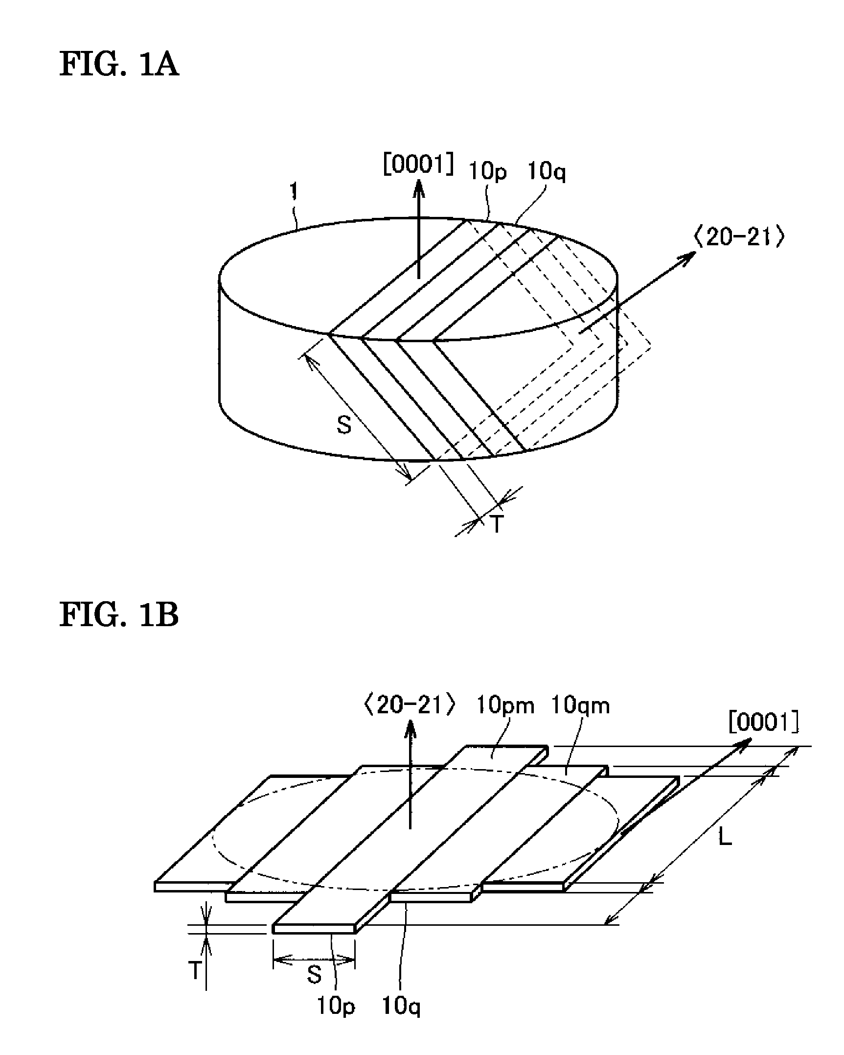
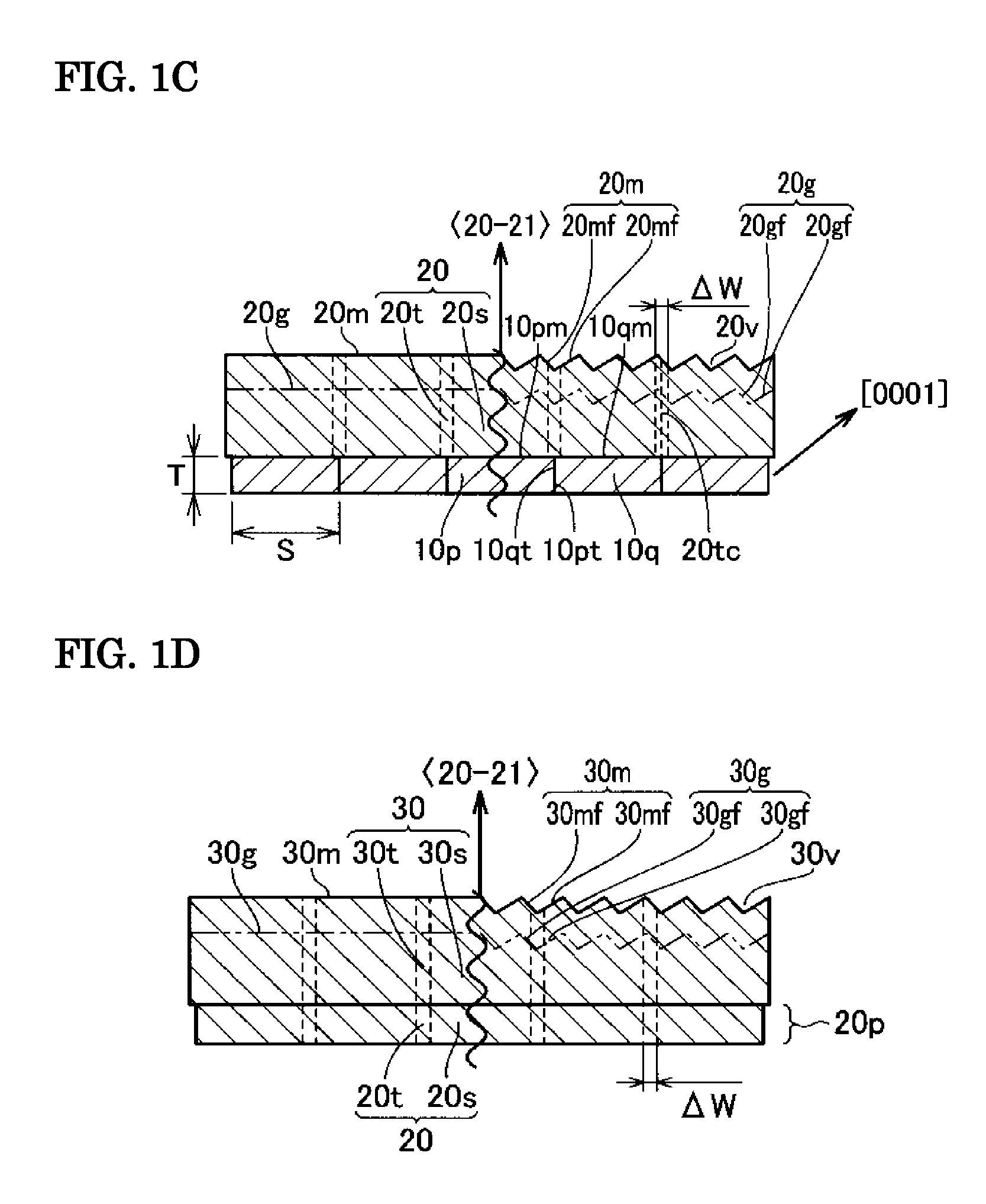
[0028]With reference to FIGS. 1 to 4, a method for producing a group III nitride crystal according to an embodiment of the present invention includes the following steps: cutting a plurality of group III nitride crystal substrates 10p and 10q having main planes 10pm and 10qm from a group III nitride bulk crystal 1, the main plane having a plane orientation with an off-angle of five degrees or less with respect to a crystal-geometrically equivalent plane orientation selected from the group consisting of {20-21}, {20-2-1}, {22-41}, and {22-4-1} (hereinafter also referred to as a substrate cutting step; see FIGS. 1A to 4A); transversely arranging the group III nitride crystal substrates 10p and 10q adjacent to each other such that the main planes 10pm and 10qm of the group III nitride crystal substrates 10p and 10q are parallel to each other and each [0001] direction of the group III nitride crystal substrates 10p and 10q is the same (hereinafter also referred to as a substrate arrangi...

second embodiment

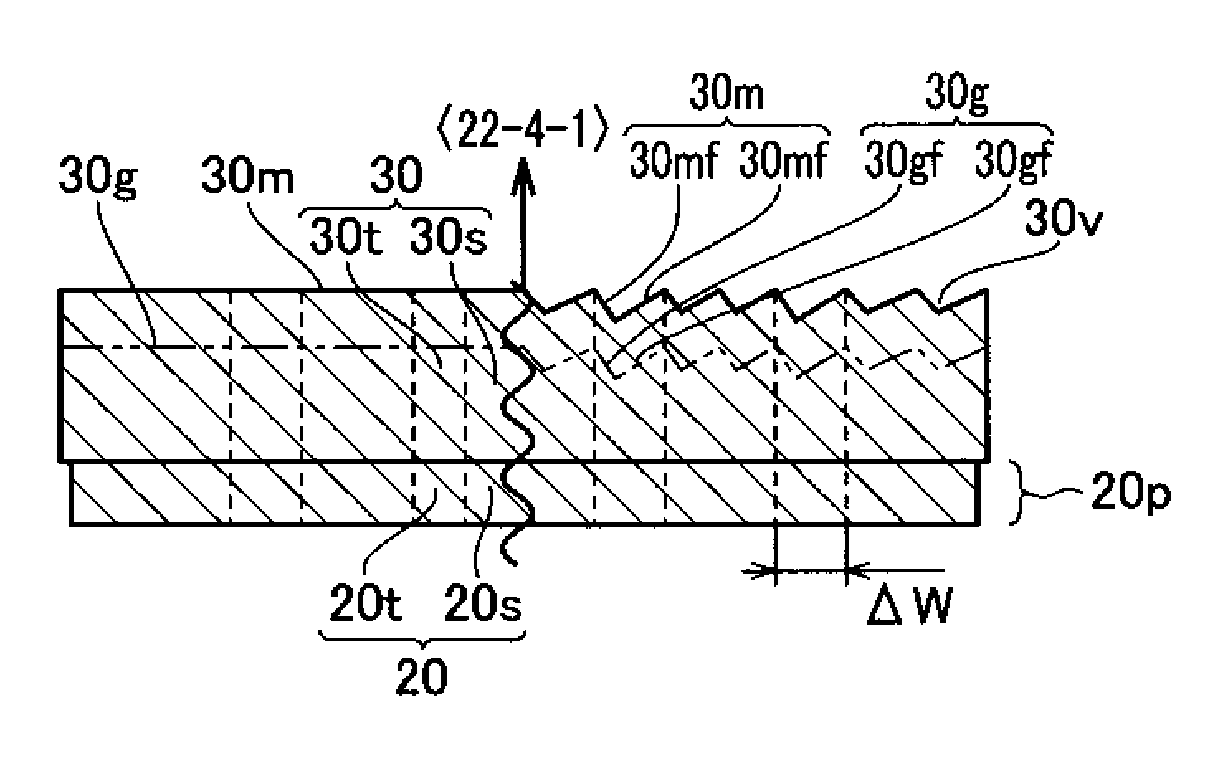
[0080]With reference to FIGS. 1 to 4, a group III nitride crystal according to another embodiment of the present invention is group III nitride crystals 20 and 30 having a main plane with a crystal-geometrically equivalent plane orientation selected from the group consisting of {20-21}, {20-2-1}, {22-41}, and {22-4-1}. The group III nitride crystals 20 and 30 have at least one of the following impurity atom concentrations: an oxygen atom concentration of 1×1016 cm−3 or more and 4×1019 cm−3 or less, a silicon atom concentration of 6×1014 cm−3 or more and 5×1018 cm−3 or less, a hydrogen atom concentration of 6×1016 cm−3 or more and 1×1018 cm−3 or less, and a carbon atom concentration of 1×1016 cm−3 or more and 1×1018 cm−3 or less.

[0081]The group III nitride crystals 20 and 30 according to the present embodiment have main planes 20m and 30m with a crystal-geometrically equivalent plane orientation selected from the group consisting of {20-21}, {20-2-1}, {22-41}, and {22-4-1}. In a ligh...

example 1

[0087]First, with reference to FIG. 1A, both main planes, a (0001) plane and a (000-1) plane, of a GaN bulk crystal (a group III nitride bulk crystal 1) were ground and polished to an average roughness Ra of 5 nm. The average surface roughness Ra was determined with AFM.

[0088]With reference to FIG. 1A, the GaN bulk crystal (the group III nitride bulk crystal 1) in which the average roughness Ra of each of the main planes was 5 nm was cut perpendicularly to the direction into a plurality of GaN crystal substrates (group III nitride crystal substrates 10p and 10q). The GaN crystal substrates had a width S of 3.1 mm, a length L in the range of 20 to 50 mm, and a thickness T of 1 mm and had a {20-21} main plane. The four planes of each of the GaN crystal substrates not yet subjected to grinding and polishing were ground and polished to an average roughness Ra of 5 nm. Thus, a plurality of GaN crystal substrates were prepared in which the average roughness Ra of the {20-21} main plane w...


PUM

PropertyMeasurementUnit
off-angleaaaaaaaaaa
roughnessaaaaaaaaaa
areaaaaaaaaaaa

Abstract

A method for producing a group III nitride crystal in the present invention includes the steps of cutting a plurality of group III nitride crystal substrates 10p and 10q having a main plane from a group III nitride bulk crystal 1, the main planes 10pm and 10qm having a plane orientation with an off-angle of five degrees or less with respect to a crystal-geometrically equivalent plane orientation selected from the group consisting of {20-21}, {20-2-1}, {22-41}, and {22-4-1}, transversely arranging the substrates 10p and 10q adjacent to each other such that the main planes 10pm and 10qm of the substrates 10p and 10q are parallel to each other and each [0001] direction of the substrates 10p and 10q coincides with each other, and growing a group III nitride crystal 20 on the main planes 10pm and 10qm of the substrates 10p and 10q.

Description

CROSS-REFERENCE TO RELATED APPLICATIONS[0001]This application is a continuation of International Application PCT / JP2010 / 059454, having an international filing date of Jun. 3, 2010, which claims the benefit of priority of Japanese patent application No. 2009-154020 filed on Jun. 29, 2009 and the benefit of priority of Japanese patent application No. 2009-204979 filed on Sep. 4, 2009, each of which is hereby incorporated by reference in their entirety.TECHNICAL FIELD[0002]The present invention relates to a group III nitride crystal and a method for producing the group III nitride crystal and also relates to a group III nitride crystal having a main plane with a plane orientation other than {0001} and a method for producing the group III nitride crystal.BACKGROUND ART[0003]Group III nitride crystals suitably used in light emitting devices, electronic devices, and semiconductor sensors are generally produced by crystal growth on a main plane of a sapphire substrate having a (0001) main ...

Claims


Application Information

Patent Timeline
Patent Type & Authority Applications(United States)
IPC IPC(8): H01L21/78C01B21/06
CPCC30B29/403H01L29/045C30B33/06H01L21/02389H01L21/0243H01L21/02433H01L21/0254H01L21/02609H01L21/0262H01L21/02658H01L33/16H01L33/32C01B21/0632C01P2002/90C01P2006/12C30B29/406
Inventor UEMATSU, KOJIOSADA, HIDEKINAKAHATA, SEIJIFUJIWARA, SHINSUKE
Owner SUMITOMO ELECTRIC IND LTD
Why Eureka
Try Eureka