Crystal growth method for nitride semiconductor and formation method for semiconductor device

a nitride semiconductor and crystal growth technology, applied in the direction of crystal growth process, polycrystalline material growth, semiconductor lasers, etc., can solve the problem of large lateral growth, improve the performance and service life of the semiconductor device, and reduce the density of dislocations

Inactive Publication Date: 2006-04-25
SONY CORP
View PDF18 Cites 88 Cited by
  • Summary
  • Abstract
  • Description
  • Claims
  • Application Information

AI Technical Summary

Benefits of technology

[0014]An advantage of the present invention is to provide a crystal growth method for a nitride semiconductor, which is capable of reducing a density of dislocations, thereby improving the performance and service life of a semiconductor device formed on a semiconductor layer produced according to an embodiment of the present invention, and to provide a method of forming a semiconductor device using the crystal growth method for a nitride semiconductor according to an embodiment of the present invention.
[0015]In an embodiment, the present invention provides a crystal growth method for a nitride semiconductor including a first crystal growth step of forming a plurality of island crystal regions of a nitride semiconductor on a base body by vapor-phase growth; and a second crystal growth step of further growing the island crystal regions while bonding boundaries of the island crystal regions to each other; wherein a crystal growth rate in the second crystal growth step is higher than a crystal growth rate in the first crystal growth step.
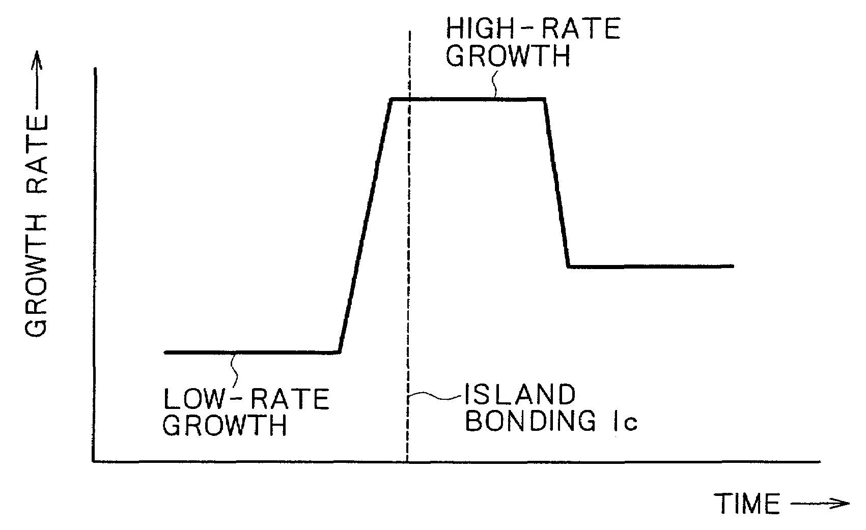
[0016]In the first crystal growth step for forming a plurality of island crystal regions of a nitride semiconductor on the base body, the island crystal regions of the nitride semiconductor can extend in the lateral direction by pseudo two-dimensional growth. In this step, since the crystal growth rate is low, the elimination of crystal from a plane parallel to the substrate becomes dominant, with a result that lateral growth becomes large. As the island crystal regions extend in the lateral direction, boundaries of the island crystal regions are bonded to each other in any suitable way. At this time, the first crystal step is shifted or changed to the second crystal step. In this shift, the crystal growth condition is modulated allowing the crystal growth rate to be increased, preferably rapidly, so as to reduce the elimination of crystal from the plane parallel to the substrate. In general, if the growth condition is changed, then crystal tends to become stable against the changed growth condition. More specifically, if the growth condition is changed, then the crystal growth direction is changed in accordance with the changed growth condition. Accordingly, in this case, the crystal growth direction is changed in accordance with the modulated crystal growth condition in such a manner that crystal is grown to bury each space between an adjacent island crystal regions. As a result, directions of dislocations in the island crystal regions are bent. This makes it possible to reduce the density of dislocations caused at the time of bonding the boundaries of the island crystal regions to each other.
[0017]In another embodiment, the present invention provides a crystal growth method for a nitride semiconductor including a first crystal growth step of forming a plurality of island crystal regions of a nitride semiconductor on a base body by vapor-phase growth; and a second crystal growth step of further growing the island crystal regions while bonding boundaries of the island crystal regions to each other; wherein a crystal growth temperature in the second crystal growth step is lower than a crystal growth temperature in the first crystal growth step.
[0018]The modulation of the crystal growth condition due to shifting of the first crystal growth step to the second crystal growth step can be realized not only by increasing the crystal growth rate but also lowering the crystal growth temperature. According to an embodiment of the crystal growth method, in the second crystal growth step, the crystal growth temperature is lowered, to reduce the elimination of crystal from the plane parallel to the substrate, thereby changing the crystal growth direction in the crystal layer, so that crystal is grown to bury each space between adjacent two of the island crystal regions. As a result, directions of dislocations in the island crystal regions are bent. This makes it possible to reduce the density of dislocations caused at the time of bonding the boundaries of the island crystal regions to each other.
[0019]In yet another embodiment, the present invention provides a crystal growth method for a nitride semiconductor including a first crystal growth step of forming a plurality of island crystal regions of a nitride semiconductor on a base body by vapor-phase growth; and a second crystal growth step of further or continued growth of the island crystal regions while bonding boundaries of the island crystal regions to each other; wherein a crystal growth rate in the second crystal growth step is higher than a crystal growth rate in the first crystal growth step or a crystal growth temperature in the second crystal step is lower than a crystal growth temperature in the first crystal growth step; and a state of irregularities on a surface of the base body is observed, and the first crystal growth step is shifted to the second crystal growth step in accordance with the state of irregularities on the surface of the base body.

Problems solved by technology

In this step, since the crystal growth rate is low, the elimination of crystal from a plane parallel to the substrate becomes dominant, with a result that lateral growth becomes large.

Method used


Image

  • Crystal growth method for nitride semiconductor and formation method for semiconductor device
  • Crystal growth method for nitride semiconductor and formation method for semiconductor device
  • Crystal growth method for nitride semiconductor and formation method for semiconductor device

Examples


Embodiment Construction

[0034]The present invention generally relates to methods of crystal growth on a semiconductor material. More specifically, the present invention relates to crystal growth methods for a nitride semiconductor, such as a gallium nitride based semiconductor and a methods for forming semiconductor devices employing crystal growth methods according to an embodiment of the present invention. The present invention can be used to make a variety of different and suitable semiconductor devices including, for example, a semiconductor light emitting device, such as a semiconductor light emitting diode, a semiconductor laser, a semiconductor transistor device or the like.

[0035]With respect to the crystal growth methods and the formation methods for a semiconductor device according to an embodiment of the present invention, a technique characterized by using a low temperature buffer, a technique characterized by selectively forming an anti-surfactant film, a technique characterized by selectively ...


PUM

PropertyMeasurementUnit
temperatureaaaaaaaaaa
crystal growth temperatureaaaaaaaaaa

Abstract

Methods of crystal growth for semiconductor materials, such as nitride semiconductors, and methods of manufacturing semiconductor devices are provided. The method of crystal growth includes forming a number of island crystal regions during a first crystal growth phase and continuing growth of the island crystal regions during a second crystal growth phase while bonding of boundaries of the island crystal regions occurs. The second crystal growth phase can include a crystal growth rate that is higher than the crystal growth rate of the first crystal growth phase and/or a temperature that is lower than the first crystal growth phase. This can reduce the density of dislocations, thereby improving the performance and service life of a semiconductor device which is formed on a nitride semiconductor made in accordance with an embodiment of the present invention.

Description

RELATED APPLICATION DATA−2 [0001]The present application claims priority to Japanese Patent Document No. P2001-113713 herein incorporated by reference to the extent permitted by law.BACKGROUND OF THE INVENTION[0002]The present invention generally relates to methods of crystal growth on a semiconductor material. More specifically, the present invention relates to crystal growth methods for a nitride semiconductor, such as a gallium nitride based semiconductor and a methods for forming semiconductor devices employing crystal growth methods of the present invention capable of fabricating a variety of semiconductor devices including, for example, a semiconductor light emitting device, such as a semiconductor light emitting diode, a semiconductor laser, a semiconductor transistor device or the like.[0003]In general, known vapor-phase growth techniques for a nitride semiconductor, such as a gallium nitride based compound semiconductor, can be problematic as it is difficult to obtain a sub...

Claims


Application Information

Patent Timeline
Patent Type & Authority Patents(United States)
IPC IPC(8): C30B25/16C23C16/34C30B25/02H01L21/20H01L21/205H01L33/12H01L33/32H01S5/323
CPCC30B25/02H01L21/0265C30B29/406H01L21/0242H01L21/02458H01L21/02513H01L21/0254H01L21/02554H01L21/02557H01L21/02565H01L21/02568H01L21/0262H01L21/02639H01L21/02647C30B29/403
Inventor BIWA, GOSHIOKUYAMA, HIROYUKIDOI, MASATOOOHATA, TOYOHARU
Owner SONY CORP
Why Eureka
Try Eureka