Substrate holding device

a technology of holding device and substrate, which is applied in the direction of semiconductor/solid-state device manufacturing, basic electric elements, electric apparatus, etc., can solve the problems of inability to monitor the state of the substrate based on the impedance, the thickness and quality of the film vary, and the temperature of the substrate is not uniform across the surface of the substra

Active Publication Date: 2013-01-03
ULVAC INC
View PDF1 Cites 20 Cited by
  • Summary
  • Abstract
  • Description
  • Claims
  • Application Information

AI Technical Summary

Benefits of technology

[0012]In view of the above-described circumstances, an object of the present invention is to provide a substrate holding device which makes it possible to grasp the warpage state

Problems solved by technology

If voltages applied to the positive and negative electrodes are fixed in the process of clamping such a warping wafer or during plasma processing, there may arise problems: for example, an alignment failure occurs due to a too weak clamping force in the process of clamping the wafer, and damage is caused due to a too strong clamping force.
As a result, the substrate temperature is non-uniform across the surface of the substrate.
When predetermined plasma processing is performed in a state in which the substrate temperature is non-uniform as described above, there is also a problem that the thickness and quality of a film vary.
Ho

Method used


Image

  • Substrate holding device
  • Substrate holding device
  • Substrate holding device

Examples


Embodiment Construction

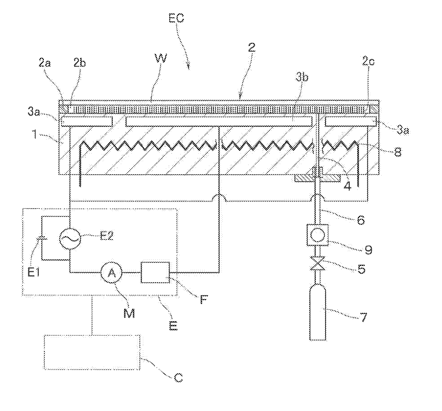
[0026]Hereinafter, referring to the drawings, a substrate holding device EC of this embodiment which is placed in a plasma processing system will be described with a substrate to be processed assumed to be a wafer W. Here, a plasma processing system in which the substrate holding device EC of this embodiment is used may be a publicly-known plasma processing system such as a DC or AC sputtering system or a reactive ion etching system irrespective of a method for producing a plasma atmosphere in the processing chamber, and therefore will not be describe in detail here.

[0027]As shown in FIG. 1, the substrate holding device EC is a so-called electrostatic chuck, and includes a chuck main body 1 placed on a bottom portion in an unillustrated processing chamber directly or with a pedestal interposed therebetween and a dielectric chuck plate 2 provided on an upper surface of the chuck main body 1. The chuck main body 1 is made of, for example, aluminum nitride, and has positive and negativ...


PUM


Abstract

A substrate holding device for clamping a substrate in a processing chamber in which plasma processing is carried out includes a chuck main body having positive and negative electrodes and, a chuck plate having a rib portion capable of bringing the peripheral edge portion of the substrate into surface contact therewith and multiple support portions provided upright and arranged at predetermined intervals in an internal space surrounded by the rib portion, a DC power supply for applying a DC voltage between the two electrodes, an AC power supply for passing an alternating current through the capacitance of the chuck plate, and first measuring means for measuring the alternating current passing through the capacitance of the chuck plate, and further includes removing means for removing an AC component superimposed on the alternating current from a plasma produced in the processing chamber during plasma processing.

Description

[0001]This application is a national phase entry under 35 U.S.C. §371 of PCT Patent Application No. PCT / JP2011 / 001557, filed on Mar. 16, 2011, which claims priority under 35 U.S.C. §119 to Japanese Patent Application No. 2010-073670, filed Mar. 26, 2010, both of which are incorporated by reference.TECHNICAL FIELD[0002]The present invention relates to a substrate holding device using an electrostatic chuck, and particularly to a substrate holding device for clamping and holding a substrate in a processing chamber in which plasma processing is carried out.BACKGROUND ART[0003]There are known techniques for obtaining a desired device structure in a semiconductor fabrication process as follows: a plasma is produced in a processing chamber in which a silicon wafer (hereinafter referred to as a “wafer”) as a substrate to be processed is placed, and plasma processing such as deposition, ion implantation, and etching is carried out on the substrate using the plasma. Such a plasma processing ...

Claims


Application Information

Patent Timeline
IPC IPC(8): H01L21/687
CPCH01L21/6831H01L21/683
Inventor MORIMOTO, NAOKIISHIDA, MASAHIKO
Owner ULVAC INC
Why Eureka
Try Eureka