METHOD AND ARCHITECTURE FOR PRE-BOND PROBING OF TSVs IN 3D STACKED INTEGRATED CIRCUITS

a technology of integrated circuits and pre-bonding, which is applied in the direction of resistance/reactance/impedence, semiconductor/solid-state device testing/measurement, instruments, etc., can solve the problems of affecting chip functionality, increasing resistance and path delay, and affecting product quality, etc., to facilitate defect localization and repair

Active Publication Date: 2013-01-03
DUKE UNIV
View PDF44 Cites 19 Cited by
  • Summary
  • Abstract
  • Description
  • Claims
  • Application Information

AI Technical Summary

Benefits of technology

[0015]Successful pre-bond defect screening in accordance with embodiments of the invention can allow defective dies to be discarded before stacking. Moreover, pre-bond testing and diagnosis can facilitate defect localization and repair prior to bonding.
[0016]According to one aspect of the invention, testing...

Problems solved by technology

As with any fabricated component, defects may occur during the manufacturing process of TSVs that can degrade product quality.
There are a number of pre-bond defects that can impact chip functionality.
These include incomplete metal filling (or microvoids) in the TSVs, which increase resistance and path delay; partial breaks in the TSV, which result in a resistive path; and complete breaks in the TSV, which result in an open path.
In addition, impurities in the TSV may also increase resistance and interconnect delay; and pinhole defects can lead to a leakage path to the substrate, with a corresponding increase in the capacitance between the TSV and the substrate.
Since methods to “unbond” die are yet to be realized, even one faulty die can cause the entire stacked IC to be discarded, including all the good dies in the stack.
The pinhole defect, as shown in FIG. 1B, may occur from uneven forming of the barrier material and causes leakage between the TSV and the substrate, increasing the TSV capacitance.
Although interest in 3D-SIC testing has surged in the past year and a number of test and design for test (DFT) solutions have been proposed, pre-bond TSV testing...

Method used


Image

  • METHOD AND ARCHITECTURE FOR PRE-BOND PROBING OF TSVs IN 3D STACKED INTEGRATED CIRCUITS
  • METHOD AND ARCHITECTURE FOR PRE-BOND PROBING OF TSVs IN 3D STACKED INTEGRATED CIRCUITS
  • METHOD AND ARCHITECTURE FOR PRE-BOND PROBING OF TSVs IN 3D STACKED INTEGRATED CIRCUITS

Examples


example

Simulation

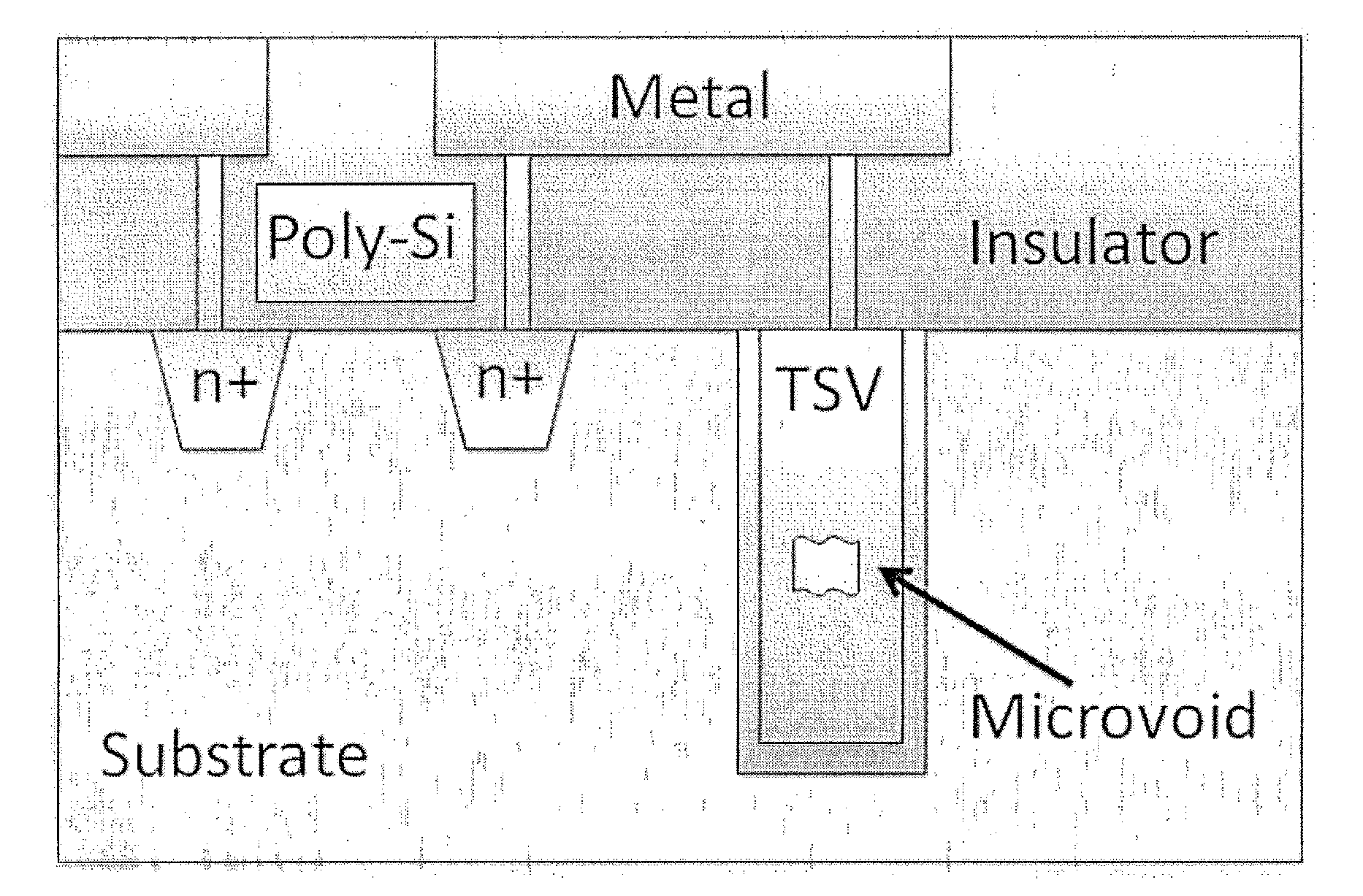
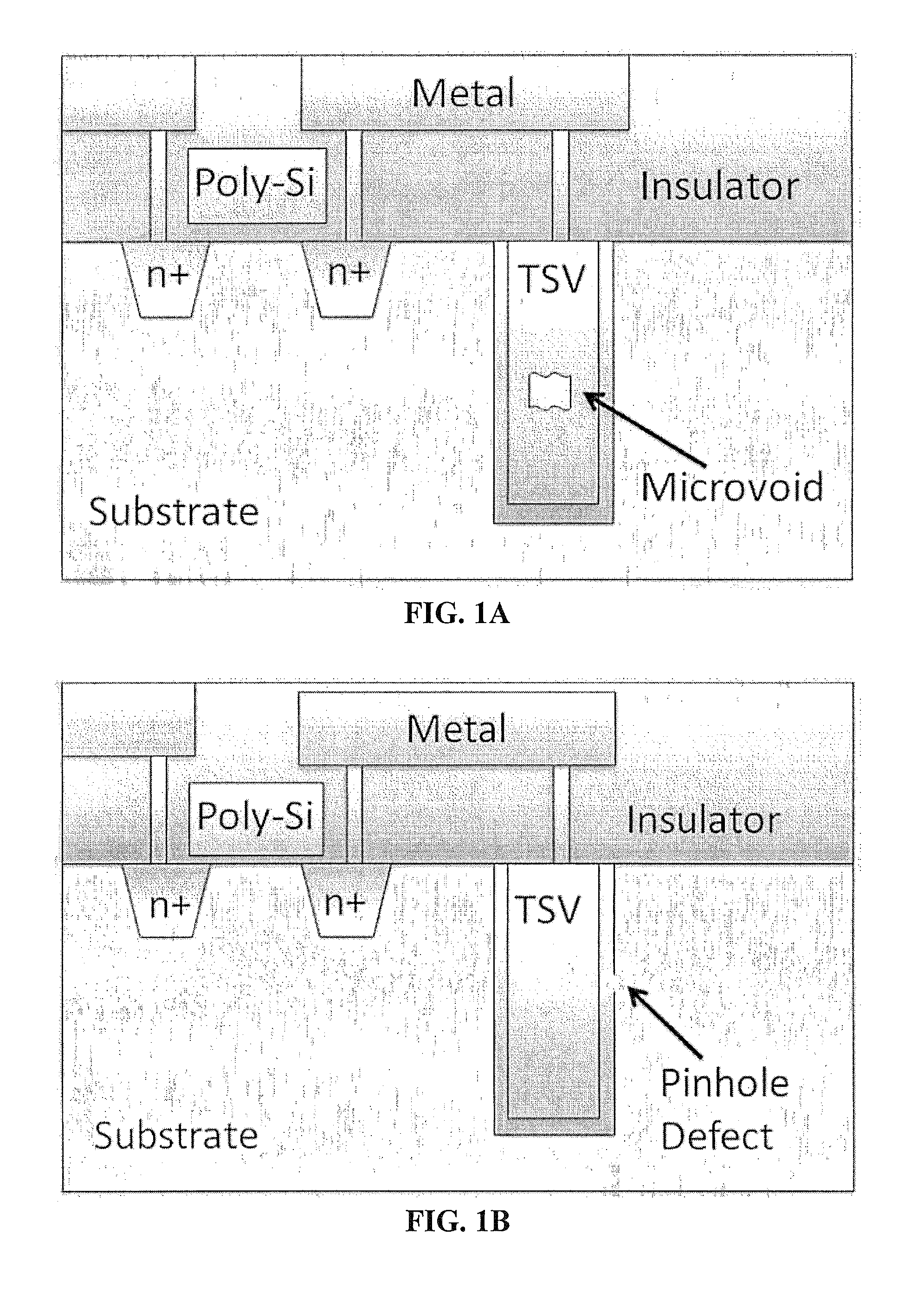
[0085]For the simulations, base line resistance and capacitance values were determined based on expected values according to the materials of the TSVs. While a TSV may be manufactured from a number of different materials, copper is often used for metal layers and polysilicon may be a non-metal alternative. The resistance of a TSV made from copper with a 2-5 μm diameter and 5 μm height is 80-200 mΩ. For a polysilicon TSV with a 28-46 μm diameter and 50 μm height, the resistance is 1.3-5.0Ω. The capacitance of a copper TSV with a 1-10 μm diameter and 30-100 μm height is 10-200 fF.

[0086]HSPICE was used to model and obtain experimental results of a TSV network of 20 TSVs. The number 20 was determined based on the relative diameter and pitch of probe leads and TSVs. Unless otherwise stated, the resistance of each TSV and contact resistance is 1Ω and the TSV's associated capacitance is 20 fF. The probe needle resistance is 10 Ω. This value is several Ohms higher than contact res...


PUM


Abstract

On-chip test architecture and design-for-testability methods for pre-bond testing of TSVs are provided. In accordance with certain embodiments of the invention, a die level wrapper is provided including gated scan flops connected to one end of each TSV. The gated scan flops include a scan flop structure and a gated output. The gated output is controlled by a signal to cause the output of the gated scan flop to either be in a “floated state” or take the value stored in the flip-flop portion of the gated scan flop. The gated output of the gated scan flop can be used to enable resistance and capacitance measurements of pre-bonded TSVs.

Description

[0001]This invention was made with government support under Grant No. CCF-1017391 awarded by the National Science Foundation. The U.S. Government has rights in this invention.BACKGROUND[0002]In an effort to produce high-performance and low-power chips, the semiconductor industry has initiated the exploration and manufacture of three-dimensional (3D) integrated circuits (ICs) based on die stacking and through-silicon-vias (TSVs). To manufacture a 3D IC, multiple dies are produced with their own active device and metal layers. Vertical TSVs are embedded in the silicon of the die wafer and connect to metal layers of the chip. The TSVs are typically in the form of a metal pillar that extends into the silicon substrate through the active device area. The TSVs may be located in or near the scribe lane, or may be in areas designated as not having an active device.[0003]After fabricating each die's TSVs and active device and metal layers, the dies are thinned through grinding, exposing the ...

Claims


Application Information

Patent Timeline
IPC IPC(8): G06F19/00G01R1/067G01R31/02
CPCG01R31/318538G01R31/318541H01L22/34G01R31/31717G01R31/2853
Inventor CHAKRABARTY, KRISHNENDUNOIA, BRANDON
Owner DUKE UNIV
Why Eureka
Try Eureka