Neutron detection using gd-loaded oxide and nitride heterojunction diodes

a heterojunction diode and neutron detection technology, which is applied in the direction of basic electric elements, electrical equipment, semiconductor devices, etc., can solve the problems of large power requirements, insufficient sensitiveness, and bulkyness, and achieve high neutron capture cross-section, superior sensitivity, and high neutron energy

Inactive Publication Date: 2013-01-10
QUANTUM DEVICES
View PDF1 Cites 9 Cited by
  • Summary
  • Abstract
  • Description
  • Claims
  • Application Information

AI Technical Summary

Benefits of technology

[0018]We have developed novel semiconducting materials and diode-like device architectures utilizing 157Gd, 10B, 6Li isotopes as the neutron absorbers. The appeal of 157Gd stems from its very high neutron capture cross-section, which remains usable at significantly higher neutron energies (up to 200-300 MeV) compared to 10B or other common absorbers. Gd containing semiconducting materials, especially when combined with B and Li detectors, require only a 2 to 4 cm moderator layer to thermalize neutron

Problems solved by technology

Generally, the commercially available neutron detectors based on 3He [1] and CdZnTe [2], [3] are not sensitive enough, are too bulky, have considerable power requirements and are too expensive to be widely applicable for fissile material interdiction operations.
This is partly because the operational devices tend to require higher voltages even for the detection of thermal neutrons.
Moreover, these devices are bulky and require more power for operation and signal generation, while at the same time have more limited lifetimes. Furthermore, it is clear that supplies of 3He are in increasingly short supply so less expensive alternatives must be sought.
A problem with this thermal neutron detection method is that neutrons emitted by fissile materials are fast, with an average energy of 1.5 MeV, while the capture cross section is greatest for slow (epithermal to thermal) neutrons.
For this reason, neutron detectors based on 3He or Cd nee

Method used


Image

  • Neutron detection using gd-loaded oxide and nitride heterojunction diodes
  • Neutron detection using gd-loaded oxide and nitride heterojunction diodes
  • Neutron detection using gd-loaded oxide and nitride heterojunction diodes

Examples


Embodiment Construction

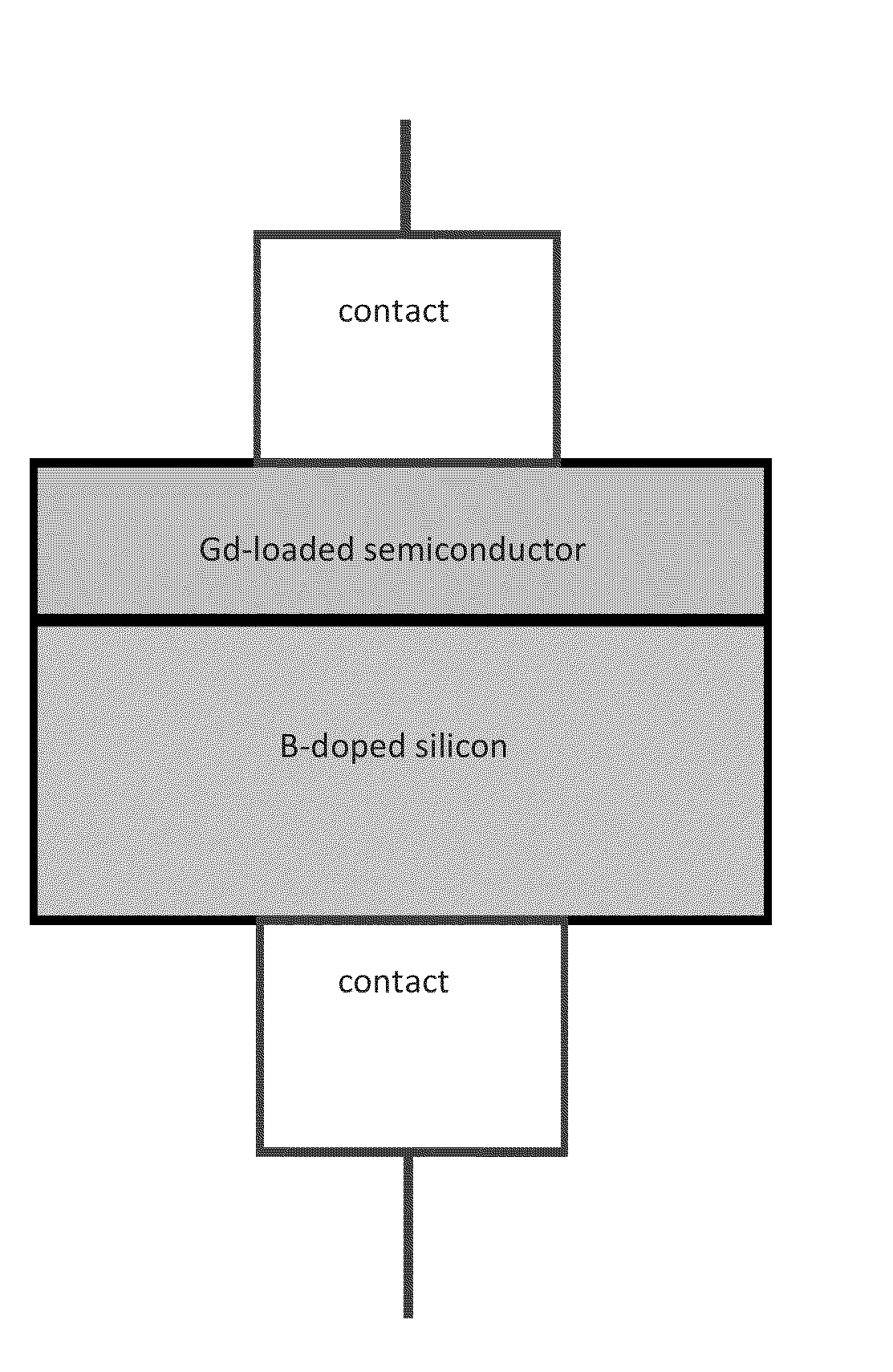
[0026]Gadolinium-doped films of GaN, and related thin films are prepared as reported in Eur. Physical J. Applied Physics 55, 3. 31303 (2011) and Eur. Physical J. Applied Physics 56, 1, 11301 (2011) incorporated herein-by-reference-for their disclosure of methods of preparing thin films of Gd-doped rare earth materials. The films of this invention can be prepared as is done for the Gd-doped GaN films. The Gd doped thin films (50-300 nm, but ideally 4-60 microns) are fabricated on an active substrate such as Si(111) or an insulating substrate such as SiO2 or sapphire Al2O3 substrates by RF plasma (EPI 620) assisted molecular beam epitaxy (MBE). The growth parameters for the deposition of Gd-doped (in situ) GaN thin films are a base pressure of 10-11 Torr, nitrogen flux of 0.75-1.0, RF power of 500 W, substrate temperature of 850-900° C., Ga cell temperature of 850° C., and Gd cell temperatures of 1050-1100° C.

[0027]The thickness of the films is measured with a surface profilometer and...


PUM


Abstract

Solid state neutron detection utilizing gadolinium as a neutron absorber is described. The new class of narrow-gap neutron-absorbing semiconducting materials, including Gd-doped HfO2, Gd-doped EuO, Gd-doped GaN, Gd2O3 and GdN are included in three types of device structures: (1) a p-n heterostructure diode with a ˜30 μm Gd-loaded semiconductor grown on a conventional semiconductor (Si or B-doped Si); (2) a p-n junction or a p-i-n trilayer diode with a Gd-loaded semiconductoron one side and single-crystal semiconducting Li2B4O7 layer on the other side of the heterojunction; and (3) a p-n junction or a p-i-n trilayer diode with a Gd-loaded semiconductoron on one side and a boron nitride (BN) semiconductor layer on the other side of the heterojunction.

Description

PRIORITY DATA AND INCORPORATION BY REFERENCE[0001]This application claims benefit of priority to U.S. Provisional Patent Application Nos. 61 / 505,223 and 61 / 505,229, both filed Jul. 7, 2011. The disclosures of both these applications are incorporated herein by reference in their entirety.BACKGROUND OF THE INVENTION[0002]1. Field of the Invention[0003]This invention generally relates to solid state neutron detectors and, more specifically, to neutron detectors made with Gd-containing oxide and nitride heterojunctions, and corresponding fabrication processes.[0004]2. Related Art[0005]There are several approaches to detecting and monitoring neutrons, including use of neutron scintillation detectors, 3He detectors, solid-state conversion layer detectors, and neutron-absorbing semiconductor solid-state detectors. In every case, neutrons are captured. Generally, the commercially available neutron detectors based on 3He [1] and CdZnTe [2], [3] are not sensitive enough, are too bulky, have c...

Claims


Application Information

Patent Timeline
IPC IPC(8): H01L31/032
CPCH01L31/0321H01L31/115H01L31/109
Inventor DOWBEN, PETER A.TANG, JINKEWISBEY, DAVID
Owner QUANTUM DEVICES
Why Eureka
Try Eureka