Film forming method and film forming apparatus

a film forming and film technology, applied in the direction of chemical vapor deposition coating, semiconductor/solid-state device details, coatings, etc., can solve the problems of diffusion of copper atoms from the copper wiring, difficult to form a film thick enough to function as a barrier, etc., to improve the adhesion of manganese-containing films, improve the film forming rate of manganese-containing films, and improve the effect of adhesion

Inactive Publication Date: 2013-01-17
TOKYO ELECTRON LTD
View PDF6 Cites 11 Cited by
  • Summary
  • Abstract
  • Description
  • Claims
  • Application Information

AI Technical Summary

Benefits of technology

[0028]In accordance with the present invention, it is possible to improve the adhesion of a manganese-containing film and form the manganese-containing film of a uniform thickness with good step coverage even in an opening. Moreover, since the film forming rate of the manganese-containing film is also improved, the manganese-containing film serving as a barrier film can be formed to have a desired film thickness. By manganese-containing film formed by the method in accordance with the present invention, it is possible to suppress the diffusion of metal such as copper into the low dielectric constant film. Therefore, it is possible to reduce the wire resistance and respond to miniaturization while ensuring the reliability of the multilayer wiring structure using the low dielectric constant film as an interlayer insulating film.

Problems solved by technology

In a case where the manganese-containing barrier film is formed by a CVD method, since the manganese-containing barrier film is hardly deposited on the low dielectric constant film, there is a problem such that it is difficult to form a film thick enough to make it function as a barrier.
Further, if the manganese-containing barrier film is formed on the porous low-k film by a CVD method, manganese may enter into the pores of the porous low-k film, thereby causing the diffusion of copper atoms from the copper wiring.

Method used


Image

  • Film forming method and film forming apparatus
  • Film forming method and film forming apparatus
  • Film forming method and film forming apparatus

Examples


first embodiment

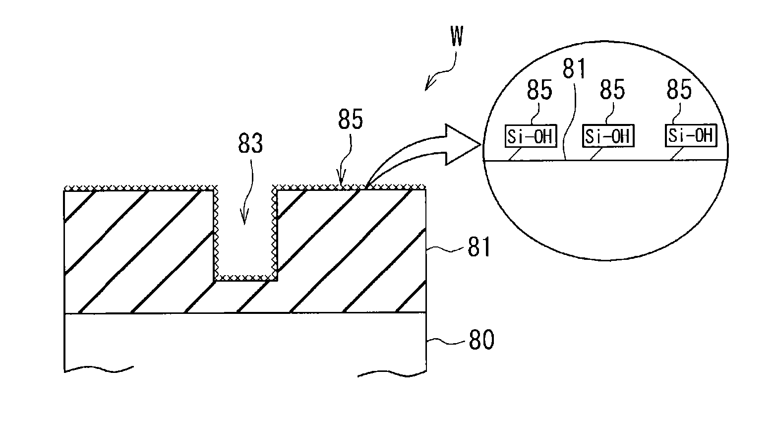
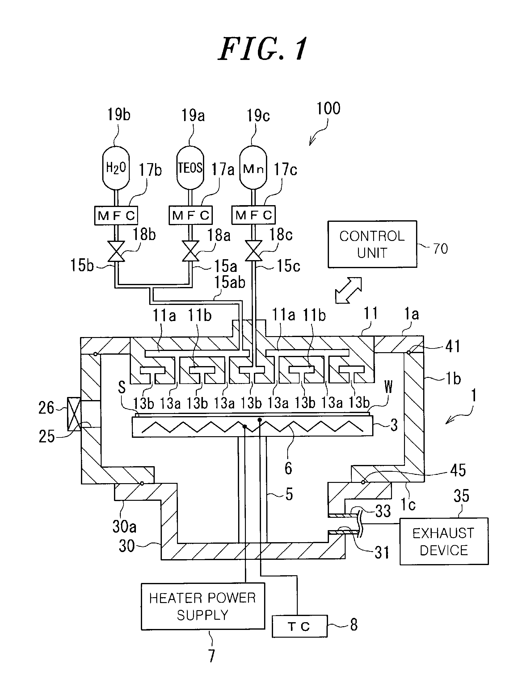
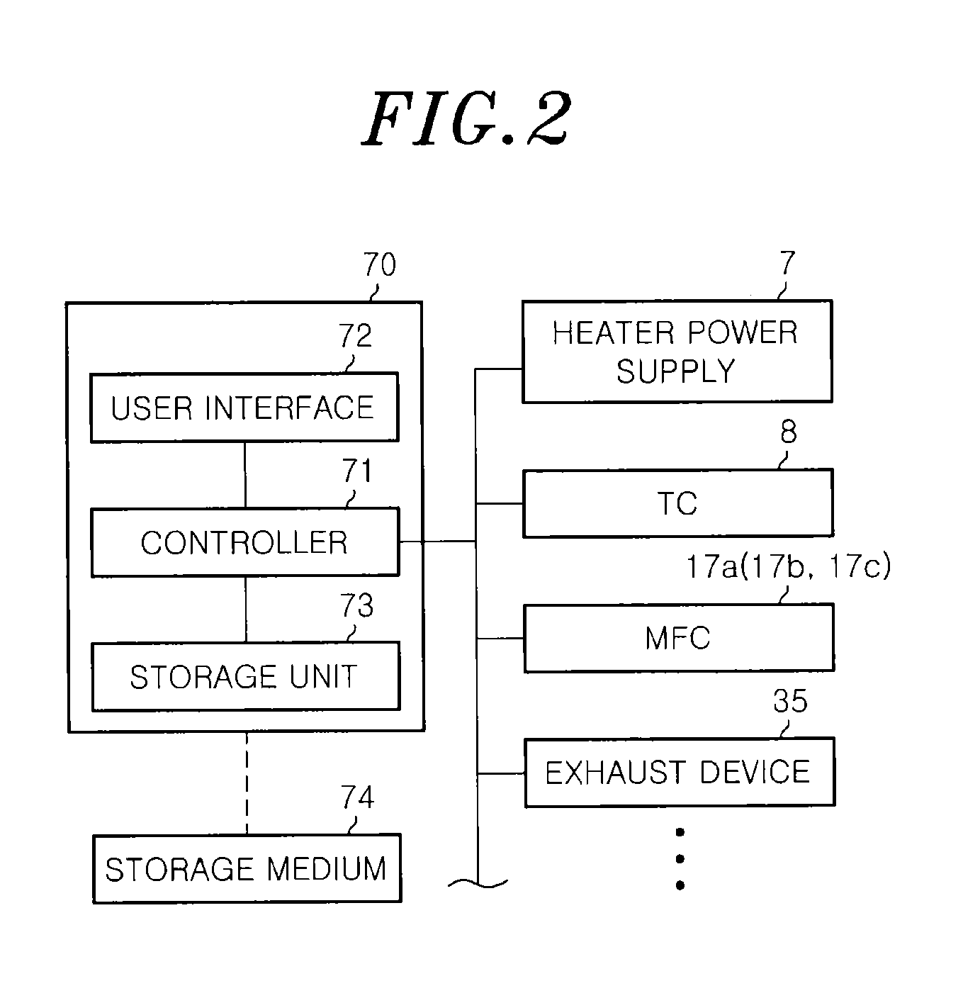
[0094]A film forming method in accordance with a first embodiment of the present invention is carried out, e.g., by performing a step of arranging an object to be processed on which an insulating film is formed in the processing chamber of the film forming apparatus, a surface modification step of supplying the Si-containing compound gas and the OH group-donating gas into the processing chamber so that Si—OH groups are formed on a surface of the insulating film, and a film forming step of supplying the film forming gas including the manganese-containing material into the processing chamber so that a manganese-containing film is formed on the surface of the insulating film on which the Si—OH groups have been formed by a CVD method. FIGS. 3 to 5 show main steps of the film forming method in accordance with the first embodiment.

[0095]

[0096]In this step, as an object to be processed, the wafer W on which the insulating film is formed is arranged in the processing chamber 1 of the film f...

second embodiment

[0116]A film forming method in accordance with a second embodiment of the present invention is carried out, e.g., by performing a step of arranging an object to be processed having an insulating film in the processing chamber of the film forming apparatus, and a film forming step of simultaneously supplying the Si-containing compound gas, the

[0117]OH group-donating gas and the film forming gas including the manganese-containing material into the processing chamber so that a manganese-containing film is formed on the surface of the insulating film by a CVD method. That is, the second embodiment is a modification example in which the surface modification step and the film forming step of the first embodiment are performed simultaneously without distinction. Thus, the following description will be made focusing on differences from the film forming method of the first embodiment, and a redundant description thereof will be omitted. Further, the description will also be made by appropria...

third embodiment

[0125]Next, a third embodiment of the present invention will be described with reference to FIGS. 9 to 17. A film forming method in accordance with the third embodiment of the present invention includes a first film forming step of forming a silicon dioxide film (SiO2 film) on a surface of the low-k film having a predetermined irregularity pattern formed on an object to be processed, and a second film forming step of forming a manganese-containing film on a surface of the silicon dioxide film by a CVD method by using the film forming gas including the manganese-containing material. FIG. 9 is a flowchart showing main steps of the film forming method of this embodiment. FIGS. 10 to 12 are views for explaining the steps. The following description will be made by using a porous low-k film as an example of the low-k film.

[0126]FIG. 10 shows a cross-sectional structure of a surface portion of the wafer W serving as an object to be processed. The base film 80 and a porous low-k film 91 whi...


PUM

PropertyMeasurementUnit
pressureaaaaaaaaaa
pressureaaaaaaaaaa
relative dielectric constantaaaaaaaaaa

Abstract

A film forming method includes a step of arranging a wafer, on which an insulating film is formed, in a processing chamber of a film forming apparatus and a surface modification step of supplying a compound gas containing silicon atoms and an OH group-donating gas into the processing chamber so that Si—OH groups are formed on the surface of the insulating film. The film forming method further includes a film forming step of supplying a film forming gas containing a manganese-containing material into the processing chamber so that a manganese-containing film is formed on the surface of the insulating film on which the Si—OH groups have been formed through a CVD method.

Description

[0001]This application is a Continuation Application of PCT International Application No. PCT / JP2011 / 055480 filed on Mar. 9, 2011, which designated the United States.FIELD OF THE INVENTION[0002]The present invention relates to a film forming method and a film forming apparatus for use in the film forming method.BACKGROUND OF THE INVENTION[0003]With a high integration of semiconductor devices and a reduction in chip size, a miniaturization of wiring and a multi-layered wiring have been developed. In the semiconductor device having a multilayer wiring structure, a propagation delay of a signal in the wiring is proportional to a product of a wire resistance R and a capacitance C between wires (RC product). Thus, in order to improve a propagation speed of the signal, it is considered to be effective to reduce the wire resistance and reduce the capacitance between wires.[0004]In order to reduce the wire resistance R, a technique of using a low-resistivity copper as a wiring material has ...

Claims


Application Information

Patent Timeline
Patent Type & Authority Applications(United States)
IPC IPC(8): C23C16/06
CPCC23C16/401H01L21/02164H01L2924/0002H01L21/02274H01L21/3105H01L21/32051H01L21/76814H01L21/76826H01L21/76831H01L21/76843H01L21/76844H01L21/0228H01L23/53238C23C16/045H01L2924/00H01L21/205
Inventor MIYOSHI, HIDENORIITOH, HITOSHISATO, HIROSHI
Owner TOKYO ELECTRON LTD
Why Eureka
Try Eureka