Nitride semiconductor light emitting element

a technology of light-emitting elements and nitride, which is applied in the manufacture of semiconductor/solid-state devices, semiconductor devices, electrical apparatus, etc., can solve the problems that the ito is not always in good ohmic contact with the semiconductor layer, and achieve the effect of low forward voltage vf and less variability of forward voltag

Inactive Publication Date: 2013-01-31
NICHIA CORP
View PDF9 Cites 4 Cited by
  • Summary
  • Abstract
  • Description
  • Claims
  • Application Information

AI Technical Summary

Benefits of technology

[0008]The present invention is made in consideration of above-mentioned problems, and an object of the present invention is to provide a nitride semiconductor light emitting element having a novel transparent electrode and a method of manufacturing the same. The nitride semiconductor light emitting element has the transparent electrode on a p-type nitride semiconductor layer, wherein the p-type nitride semiconductor layer and the transparent electrode can be in good ohmic contact with each other and wherein the variability of the forward voltage (Vf) among a plurality of light emitting elements made from the same wafer can be reduced.
[0017]According to the nitride semiconductor light emitting element of the invention and the method of manufacturing the same, it is possible to provide the nitride semiconductor light emitting element which has a low forward voltage Vf and has less variability of the forward voltage (among a plurality of light emitting elements made from the same wafer).

Problems solved by technology

However, ITO is not always in good ohmic contact with a semiconductor layer since ITO exhibits an n-type semiconductor property.

Method used


Image

  • Nitride semiconductor light emitting element
  • Nitride semiconductor light emitting element

Examples


example 1

[0072]For purpose of evaluation of the variability of Vf, a plurality of nitride semiconductor light emitting elements was manufactured at the same time.

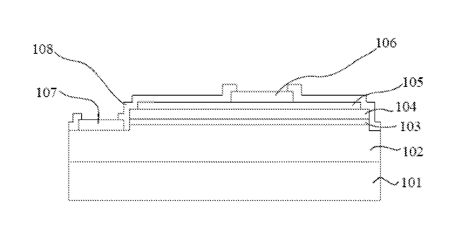
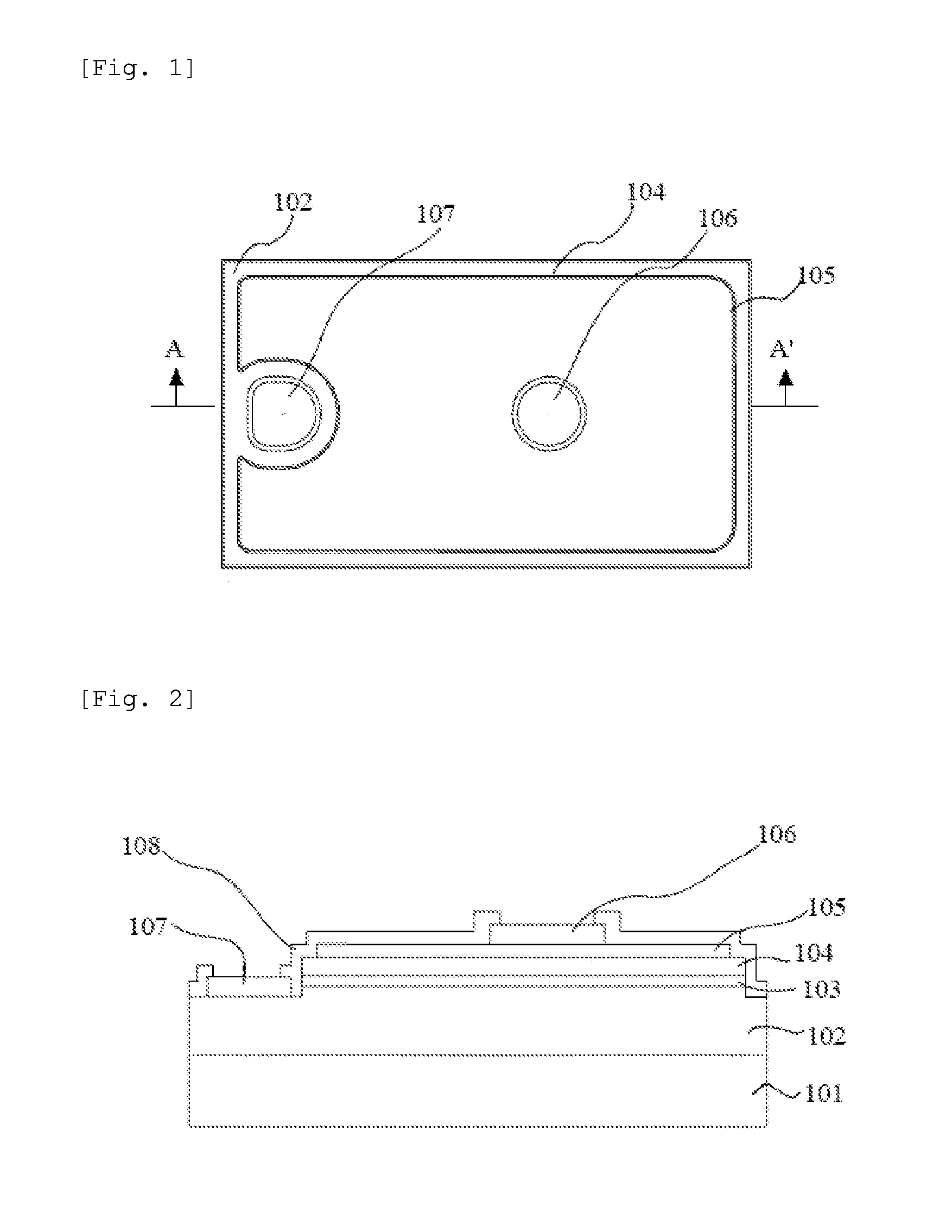
[0073]The n-side nitride semiconductor layer 102, the light emitting layer 103 and the p-side nitride semiconductor layer 104 were stacked on a sapphire substrate 101 with 2 inch diameter via a AlGaN buffer layer.

[0074]The n-side nitride semiconductor layer 102 was formed by stacking undoped GaN (1.5 μm), Si doped GaN (4.2 μm), undoped GaN (0.15 μm), Si doped GaN (0.01 μm), undoped Can (0.15 μm), Si doped GaN (0.03 μm), undoped GaN (5 nm), and a super lattice layer (120 nm) in which GaN and InGaN were twenty times repeatedly stacked and finally GaN was stacked in this order.

[0075]The light emitting layer 103 was formed by repeatedly stacking six times GaN (8 nm) and InGaN (3 nm) and finally stacking GaN (8 nm). The first stacked GaN layer was doped with Si, and the finally stacked GaN layer was not doped.

[0076]The p-side nitride sem...

example 2

[0089]An effect of annealing conditions of the transparent electrode 105 on the forward voltage Vf was evaluated.

[0090]This example was different from Example 1 in that measurement was carried out after dividing the wafer into chips. Other than that was the same as Example 1.

[0091]As the same for Example 1, the n-side nitride semiconductor layer 102, the light emitting layer 103 and the p-side nitride semiconductor layer 104 were stacked, and the transparent electrode 105 was formed.

[0092]The transparent electrode 105 having the thickness of 170 nm was formed under Ar atmosphere by the sputtering method using the target comprising indium oxide containing Ge and Si.

[0093]After forming the transparent electrode 105, the nitride semiconductor light emitting element was annealed. The annealing conditions (the annealing temperature, the annealing atmosphere and the annealing pressure) were listed in Tables 1 and 2.

[0094]As the same for Example 1, the n-side pad electrode 107, the p-side ...

example 3

[0098]An effect of film forming conditions and the annealing conditions of the transparent electrode 105 on the ohmic contact was evaluated.

[0099]This example was different from Example 1 in the film forming conditions of the transparent electrode 105. Furthermore, this example was different from Example 1 in that measurement was carried out after dividing the wafer into chips. Other than that was the same as Example 1.

[0100]As the same for Example 1, the n-side nitride semiconductor layer 102, the light emitting layer 103 and the p-side nitride semiconductor layer 104 were stacked, and the transparent electrode 105 was formed.

[0101]The transparent electrode 105 having the thickness of 170 nm was formed by the sputtering method using the target comprising indium oxide containing Ge and Si. The samples were formed under different atmospheres in the sputtering device during film forming. The atmosphere for each sample was, Ar only (sample Nos. 13 and 16-19); Ar and O2 (Ar flow rate: 6...


PUM


Abstract

An object of the present invention is to provide a nitride semiconductor light emitting element having a novel transparent electrode. The nitride semiconductor light emitting element has the transparent electrode on a p-type nitride semiconductor layer, wherein the p-type nitride semiconductor layer and the transparent electrode can be in good ohmic contact to each other and wherein the variability of the forward voltage (Vf) within the wafer can be reduced.The present invention is a nitride semiconductor light emitting element including: an n-side nitride semiconductor layer; a p-side nitride semiconductor layer; and a transparent electrode formed on the p-side nitride semiconductor layer, wherein the transparent electrode is made of indium oxide containing Ge and Si.

Description

REFERENCE TO RELATED APPLICATIONS[0001]This application is a national stage application under USC 371 of International Application No. PCT / JP2011 / 056976, filed Mar. 23, 2011, which claims the priority of Japanese Patent Application No. 2010-066737, filed Mar. 23, 2010, the entire contents of which are incorporated herein by reference.FIELD OF THE INVENTION[0002]The present invention relates to a nitride semiconductor light emitting element having a transparent conductive oxide film as an electrode.BACKGROUND OF THE INVENTION[0003]Conventionally, a nitride semiconductor light emitting element structure in which a p-type semiconductor layer and an n-type semiconductor layer are stacked on a substrate and electrodes electrically connected to the p-type and n-type semiconductor layers respectively are formed is known. Furthermore, a structure of the electrode electrically connected to the p-type semiconductor in which an electrode made of a transparent material is formed on a whole surf...

Claims


Application Information

Patent Timeline
Patent Type & Authority Applications(United States)
IPC IPC(8): H01L33/02H01L33/62
CPCH01L33/0095H01L2933/0016H01L33/42H01L33/32H01L33/007H01L33/0075H01L33/36H01L33/40
Inventor MUSASHI, NAOKI
Owner NICHIA CORP
Why Eureka
Try Eureka