Light emitting diode and manufacturing method thereof

a technology of light-emitting diodes and manufacturing methods, which is applied in the direction of semiconductor/solid-state device manufacturing, electrical apparatus, semiconductor devices, etc., can solve the problems of reducing the light-emitting efficiency of leds, adding processing time, manpower and more manufacturing costs

Inactive Publication Date: 2013-02-07
SCIENBIZIP CONSULTINGSHENZHENCO
View PDF6 Cites 6 Cited by
  • Summary
  • Abstract
  • Description
  • Claims
  • Application Information

AI Technical Summary

Benefits of technology

[0002]LEDs have low power consumption, high efficiency, quick reaction time, long lifetime, and the absence of toxic elements such as mercury during manufacturing. Many LEDs comprise a sapphire and an epitaxial layer disposed on the sapphire. An active layer (or a light emitting layer) located inside the epitaxial layer is configured for emitting light; however, the other layers of the epitaxial layer or the sapphire may absorb the emitted light to reduce a light emitting efficiency of the LED. The epitaxial layer and the sapphire have high refractive indexes, which is about 1.6˜2.6, such that total reflections of the emitted light inside the LED may result in the useful light output being reduced. For solving foresaid limitations, an LED with roughened surfaces may be configured to make an LED having rough lateral surfaces, for which photo-enhancing chemical wet etching method (PEC) and an etchant such as potassium hydroxide (K.OH) may be used. However, such manufacturing method may add extra processing time, manpower and more manufacturing cost. Therefore, a new LED and its manufacturing method that overcome aforementioned deficiencies are required.

Problems solved by technology

An active layer (or a light emitting layer) located inside the epitaxial layer is configured for emitting light; however, the other layers of the epitaxial layer or the sapphire may absorb the emitted light to reduce a light emitting efficiency of the LED.
However, such manufacturing method may add extra processing time, manpower and more manufacturing cost.

Method used


Image

  • Light emitting diode and manufacturing method thereof
  • Light emitting diode and manufacturing method thereof
  • Light emitting diode and manufacturing method thereof

Examples


Embodiment Construction

[0009]Exemplary embodiments of the disclosure will be described with reference to the accompanying drawings.

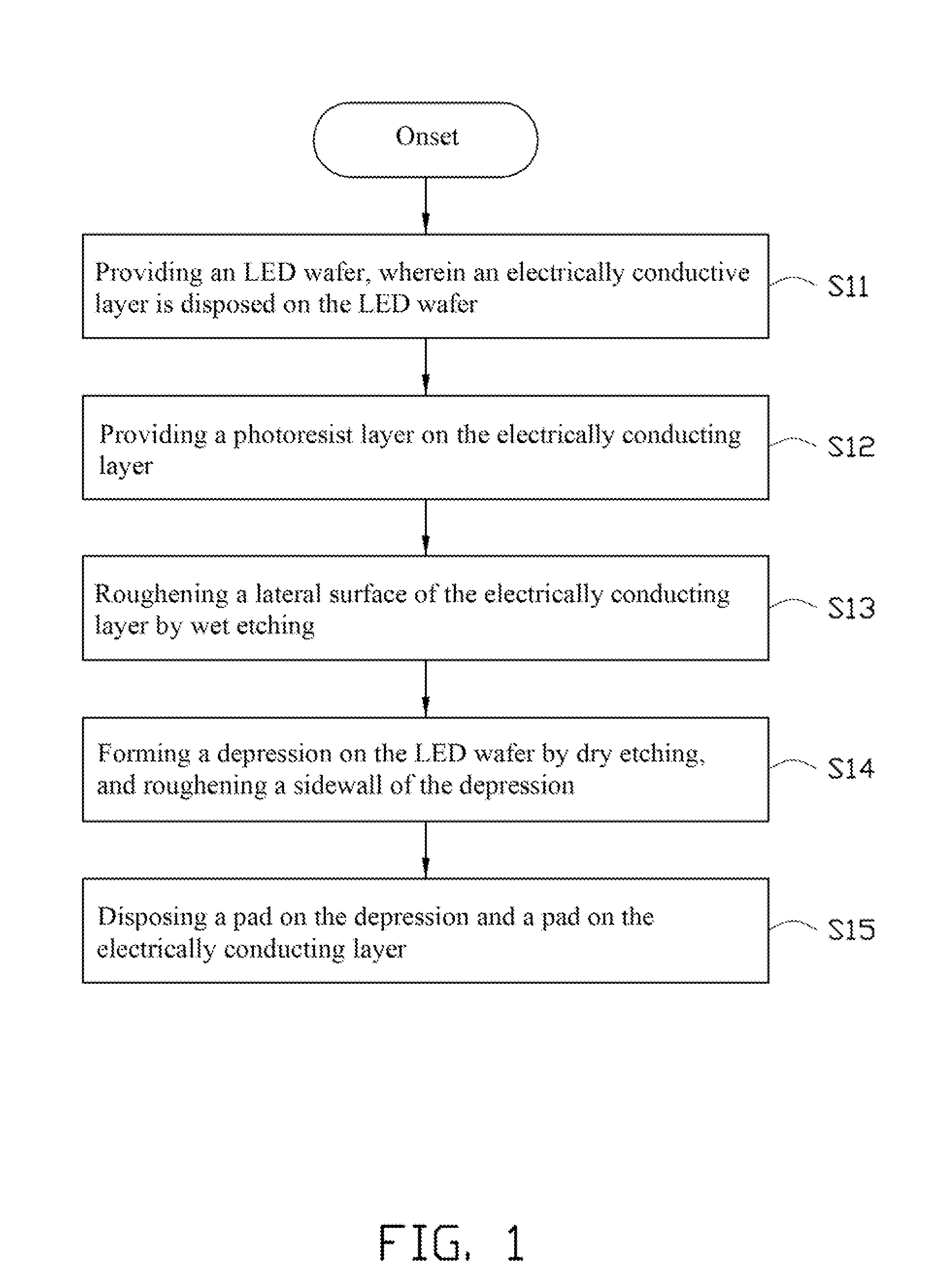
[0010]Referring to FIG. 1, the present disclosure provides a manufacturing method for an LED, comprising following steps:

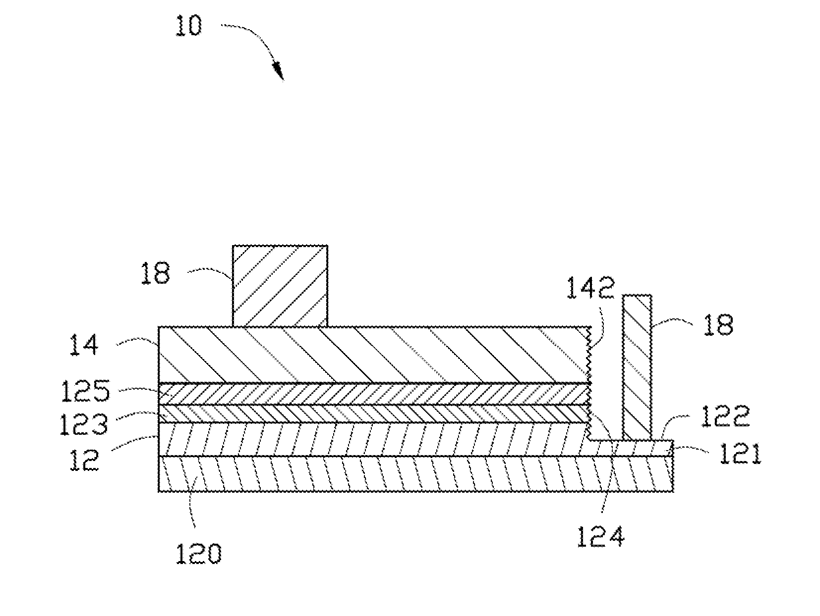
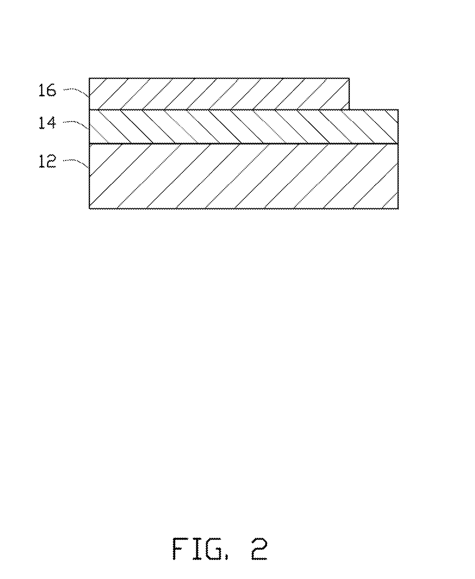
[0011]In step S11, an LED wafer 12 is provided, wherein an electrically conductive layer 14 is disposed on the LED wafer 12, as shown in FIG. 2. In the embodiment, the LED wafer 12 comprises a substrate 120 and an epitaxial layer on the substrate 120. The epitaxial layer comprises an N-type epitaxial layer 121 on the substrate 120, a light emitting layer 123 on the N-type epitaxial layer 121 and a P-type epitaxial layer 125 on the light emitting layer 123. The electrically conductive layer 14 is on the P-type epitaxial layer 125 of the LED wafer 12. The electrically conductive layer 14 can be made by vapor deposition, and be composed of indium tin oxide (ITO). The substrate 120 can be sapphire, silicon carbide (SiC) or gallium nitride (GaN). The LED wafer 12...


PUM


Abstract

A manufacturing method for an LED with roughened lateral surfaces comprises following steps: providing an LED wafer with an electrically conductive layer disposed thereon; providing a photoresist layer on the electrically conductive layer; roughening a lateral surface of the electrically conductive layer by wet etching; forming a depression in the LED wafer by dry etching and roughening a sidewall of the LED wafer defining the depression; and disposing two pads respectively in the depression and the conducting layer. The disclosure also provides an LED with roughened lateral surfaces. A roughness of the roughened lateral surfaces is measurable in micrometers.

Description

TECHNICAL FIELD[0001]The disclosure relates to light emitting diodes (LEDs) and the manufacturing method thereof, and more particularly to an LED having roughened lateral surfaces.DESCRIPTION OF THE RELATED ART[0002]LEDs have low power consumption, high efficiency, quick reaction time, long lifetime, and the absence of toxic elements such as mercury during manufacturing. Many LEDs comprise a sapphire and an epitaxial layer disposed on the sapphire. An active layer (or a light emitting layer) located inside the epitaxial layer is configured for emitting light; however, the other layers of the epitaxial layer or the sapphire may absorb the emitted light to reduce a light emitting efficiency of the LED. The epitaxial layer and the sapphire have high refractive indexes, which is about 1.6˜2.6, such that total reflections of the emitted light inside the LED may result in the useful light output being reduced. For solving foresaid limitations, an LED with roughened surfaces may be configu...

Claims


Application Information

Patent Timeline
Patent Type & Authority Applications(United States)
IPC IPC(8): H01L33/22H01L33/32
CPCH01L33/007H01L33/22H01L33/24H01L2933/0016H01L33/40H01L33/42H01L33/32
Inventor SHEN, CHIA-HUIHUNG, TZU-CHIEN
Owner SCIENBIZIP CONSULTINGSHENZHENCO
Why Eureka
Try Eureka