Semiconductor device member, production method of semiconductor-device-member formation liquid and semiconductor device member, and semiconductor-device-member formation liquid, phosphor composition, semiconductor light-emitting device, lighting system and image display system using the same

a semiconductor and semiconductor technology, applied in the direction of semiconductor/solid-state device details, luminescent compositions, chemistry apparatus and processes, etc., can solve the problems of low adhesion, degradation of phosphor or luminous elements, and difficulty in using a semiconductor light-emitting device generally as a power device, so as to improve the performance of the semiconductor device and maintain the performance. , the effect of film-forming ability and adhesion

Inactive Publication Date: 2013-02-14
MITSUBISHI CHEM CORP
View PDF4 Cites 20 Cited by
  • Summary
  • Abstract
  • Description
  • Claims
  • Application Information

AI Technical Summary

Benefits of technology

[0062]The semiconductor device member of the present invention is superior in heat resistance, light resistance, film-formation capability and adhesion, and capable of sealing a semiconductor device without causing cracks or peelings even after used for a long period of time. Usually, it can be applied in a thicker film state than the previous inorganic semiconductor device member. It can easily seal the semiconductor device and hold the phosphor just by applying it on the semiconductor device and drying it.
[0063]With the semiconductor-device-member formation liquid and the phosphor composition of the present invention, the semiconductor device member of the present invention can be produced.
[0064]By the production methods of the semiconductor-device-member formation liquid and the semiconductor device member of the present invention, the semiconductor-device-member formation liquid and the semiconductor device member of the present invention can be produced.
[0065]The semiconductor light-emitting device of the present invention can maintain its performance for a long period of time without causing cracks, peelings or colorings even after used for a long time, because the sealant thereof is superior in heat resistance, light resistance, film-formation capability and adhesion.

Problems solved by technology

However, it has been difficult to use a semiconductor light-emitting device generally as power device.
If the LED chip is upsized, for the purpose of preventing increase in heat density, there will be unevenness in thermal expansion coefficients of the sealant and the chip, leading to low adhesion, as peeling of the sealant from the chip.
However, due to high hygroscopicity of epoxy resin, there have been problems of cracks caused by heat from the semiconductor element when the semiconductor device is used for a long time and degradation of the phosphor or the luminous element caused by moisture infiltration.
Also in recent years, with shortening of the luminous wavelength, there has been a problem of dramatic decrease in brightness of the semiconductor device because the epoxy resin degrades and colors when the device is used illuminated for a long time at a high output level.
However, silicone resin does not yet have sufficient adhesion, transparency and weather resistance.

Method used


Image

  • Semiconductor device member, production method of semiconductor-device-member formation liquid and semiconductor device member, and semiconductor-device-member formation liquid, phosphor composition, semiconductor light-emitting device, lighting system and image display system using the same
  • Semiconductor device member, production method of semiconductor-device-member formation liquid and semiconductor device member, and semiconductor-device-member formation liquid, phosphor composition, semiconductor light-emitting device, lighting system and image display system using the same
  • Semiconductor device member, production method of semiconductor-device-member formation liquid and semiconductor device member, and semiconductor-device-member formation liquid, phosphor composition, semiconductor light-emitting device, lighting system and image display system using the same

Examples


embodiments

[5-5] Embodiments

A. Embodiments that do not Use Fluorescence

embodiment a-1

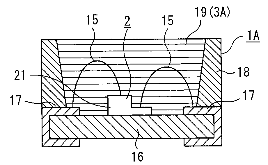
[0603]In light emitting device 1A of the present embodiment, as shown in FIG. 1, luminous element 2 is surface-mounted on an insulating substrate 16 on which printed wiring 17 is carried out. In luminous element 2, a p-type semiconductor layer (not shown) and an n-type semiconductor layer (not shown) in a luminous layer part 21 are connected electrically to printed wirings 17 and 17 via conductive wires 15 and 15 respectively. Conductive wires 15 and 15 have a small cross section so that the light emitted from luminous element 2 may not be blocked.

[0604]As luminous element 2, one that emits light of any wavelengths, from ultraviolet to infrared regions, may be used. In this embodiment, a gallium nitride LED chip is assumed to be used. In luminous element 2, an n-type semiconductor layer (not shown) is formed on the lower side in FIG. 1 and a p-type semiconductor layer (not shown) is formed on the upper side in the same. The upper side of FIG. 1 is assumed to be the front side in the...

embodiment a-2

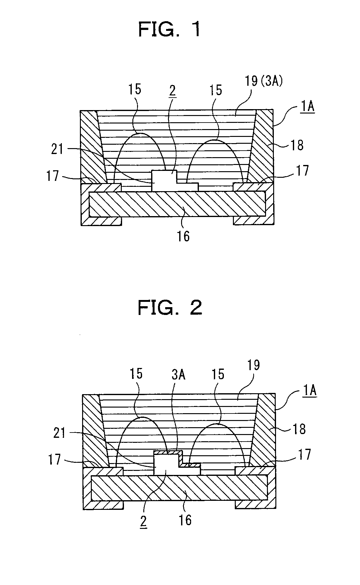
[0608]Light emitting device 1A of the present embodiment is structured, as shown in FIG. 2, in the same manner as the above embodiment A-1, except that the front side of luminous element 2 is covered with transparent member 3A and sealing part 19, formed on member 3A. Sealing part 19 is formed of a material different from that of transparent member 3A. Transparent member 3A on the surface of luminous element 2 is a transparent thin film, functioning as a light extracting film and sealing film. Transparent member 3A can be formed, for example, by coating the above liquid for forming the semiconductor light-emitting device member, by a method of spin coating or the like, during the formation process of a chip of luminous element 2. Meanwhile, the same components as in embodiment A-1 are designated by the same reference numerals to omit redundant explanations.

[0609]Thus, because light emitting device 1A of the present embodiment is also provided with luminous element 2 and transparent ...


PUM

PropertyMeasurementUnit
viscosityaaaaaaaaaa
viscosityaaaaaaaaaa
cure temperatureaaaaaaaaaa

Abstract

To provide a semiconductor device member that is superior in heat resistance, light resistance, film-formation capability and adhesion, and is capable of sealing a semiconductor device and holding a phosphor without causing cracks, peelings and colorings even after used for a long period of time, the weight loss at the time of heating, measured by a predetermined weight-loss at-the-time-of-heating measurement method, is 50 weight % or lower and the ratio of peeling, measured by a predetermined adhesion evaluation method, is 30% or lower, in the semiconductor device member.

Description

CROSS REFERENCE TO RELATED APPLICATION[0001]This application is a continuation application of U.S. application Ser. No. 12 / 438,283, filed on Apr. 2, 2009, which is a 371 of PCT / JP07 / 66310, filed on Aug. 27, 2007, and claims priority to the following applications: Japanese Patent Application No. 2006-225410, filed on Aug. 22, 2006.TECHNICAL FIELD[0002]The present invention relates to a novel semiconductor device member, to a production method of a semiconductor-device-member formation liquid and a semiconductor device member, and to a semiconductor light-emitting device, a semiconductor-device-member formation liquid and a phosphor composition. More specifically, the present invention relates to a semiconductor device member that is superior in heat resistance, light resistance, film-formation capability and adhesion, to a production method of a semiconductor-device-member formation liquid and a semiconductor device member, and to a semiconductor light-emitting device with a large-si...

Claims


Application Information

Patent Timeline
Patent Type & Authority Applications(United States)
IPC IPC(8): C08G77/08C09K11/08C08L83/06H01L23/29H01L23/31H01L33/32H01L33/48H01L33/50H01L33/56H01L33/62
CPCC09K11/7721H01L2924/12041C09K11/7735C09K11/7738C09K11/774C09K11/7774C09K11/7775C09K11/7781C09K11/7789C09K11/7794C09K11/7795H01L23/24H01L23/293H01L33/507H01L33/54H01L33/58H01L2224/48091H01L2224/48227H01L2224/48247H01L2224/49107H01L2224/73265H01L2924/01004H01L2924/01012H01L2924/0102H01L2924/01025H01L2924/01046H01L2924/01057H01L2924/01063H01L2924/01077H01L2924/01078H01L2924/01079H01L2924/19041C09K11/7734H01L2224/32245H01L2924/01019H01L2924/01021H01L2924/01066H01L2924/01067H01L2924/01068H01L2924/01322H01L2224/45144H01L2224/48257H01L2924/10253H01L2224/32257H01L24/17H01L2224/8592H01L2924/00014H01L2924/00H01L2924/181H01L2924/12042H01L2924/00012H01L23/29C09K11/73C09K11/77H01L33/56
Inventor KATO, HANAKOMORI, YUTAKAKOBAYASHITOMURA, TSUBASA
Owner MITSUBISHI CHEM CORP
Why Eureka
Try Eureka